Catalog
CMOS Programmable Timer
Key Features
• 24 flip-flop stages - - counts from 20to 224Last 16 stages selectable by BCD select codeBypass input allows bypassing first 8 stagesOn-chip RC oscillator provisionClock inhibit inputSchmitt-trigger in clock line permits operation with very long rise and fall timesOn-chip monostable output provisionTypical fCL= 3 MHz at VDD= 10 VTest mode allows fast test sequenceSet and reset inputsCapable of driving two low power TTL loads, one lower-power Schottky load, or two HTL loads over the rated temperature rangeStandardized, symmetrical output characteristics100% tested for quiescent current at 20 V5-V, 10-V, and 15-V parametric ratingsMeets all requirements of JEDEC Tentative Standard No. 13B, "Standard Specifications for Description of ’B’ Series CMOS Devices"24 flip-flop stages - - counts from 20to 224Last 16 stages selectable by BCD select codeBypass input allows bypassing first 8 stagesOn-chip RC oscillator provisionClock inhibit inputSchmitt-trigger in clock line permits operation with very long rise and fall timesOn-chip monostable output provisionTypical fCL= 3 MHz at VDD= 10 VTest mode allows fast test sequenceSet and reset inputsCapable of driving two low power TTL loads, one lower-power Schottky load, or two HTL loads over the rated temperature rangeStandardized, symmetrical output characteristics100% tested for quiescent current at 20 V5-V, 10-V, and 15-V parametric ratingsMeets all requirements of JEDEC Tentative Standard No. 13B, "Standard Specifications for Description of ’B’ Series CMOS Devices"
Description
AI
CD4536B is a programmable timer consisting of 24 ripple-binary counter stages. The salient feature of this device is its flexibility. The device can count from 1 to 224or the first 8 stages can be bypassed to allow an output, selectable by a 4-bit code, from any one of the remaining 16 stages. It can be driven by an external clock or an RC oscillator that can be constructed using on-chip components. Input IN1 serves as either the external clock input or the input to the on-chip RC oscillator. OUT1 and OUT2 are connection terminals for the external RC components. In addition, an on-chip monostable circuit is provided to allow a variable pulse width output. Various timing functions can be achieved using combinations of these capabilities.
A logic 1 on the 8-BYPASS input enables a bypass of the first 8 stages and makes stage 9 the first counter stage of the last 16 stages. Selection of 1 of 16 outputs is accomplished by the decoder and the BCD inputs A, B, C and D. MONO IN is the timing input for the on-chip monostable oscillator. Grounding of the MONO IN terminal through a resistor of 10K ohms or higher, disables the one-shot circuit and connects the decoder directly to the DECODE OUT terminal. A resistor to VDDand a capacitor to ground from the MONO IN terminal enables the one-shot circuit and control its pulse width.
A fast test mode is enabled by a logic 1 on 8-BYPASS, SET, and RESET. This mode divides the 24-stage counter into three 8-stage sections to facilitate a fast test sequence.
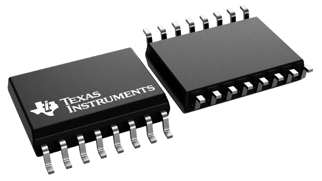
The CD4536B types are supplied in 16-lead hermetic dual-in-line ceramic packages (F3A suffix), 16-lead dual-in-line plastic packages (E suffix), 16-lead small-outline packages (DW, DWR, and NSR suffixes), and 16-lead thin shrink small-outline packages (PW and PWR suffixes).


