Catalog
8-ch, 2-V to 6-V buffers with 3-state outputs
Key Features
• ’HC540, CD74HCT540: inverting’HC541, ’HCT541: non-invertingBuffered inputsThree-state outputsBus line driving capabilityTypical propagation delay = 9 ns at VCC= 5 V, CL= 15 pF, TA= 25℃Fanout (over temperature range)Standard outputs: 10 LSTTL loadsBus driver outputs: 15 LSTTL loadsWide operating temperature range: –55℃ to 125℃Balanced propagation delay and transition timesSignificant power reduction compared to LSTTL Logic ICsHC types2 V to 6 V operationHigh noise immunity: NIL= 30%, NIH= 30% of VCCat VCC= 5 VHCT types4.5 V to 5.5 V operationDirect LSTTL input logic compatibility, VIL= 0.8 V (max), VIH= 2 V (min)CMOS input compatibility, II≤ 1 µA at VOL, VOH’HC540, CD74HCT540: inverting’HC541, ’HCT541: non-invertingBuffered inputsThree-state outputsBus line driving capabilityTypical propagation delay = 9 ns at VCC= 5 V, CL= 15 pF, TA= 25℃Fanout (over temperature range)Standard outputs: 10 LSTTL loadsBus driver outputs: 15 LSTTL loadsWide operating temperature range: –55℃ to 125℃Balanced propagation delay and transition timesSignificant power reduction compared to LSTTL Logic ICsHC types2 V to 6 V operationHigh noise immunity: NIL= 30%, NIH= 30% of VCCat VCC= 5 VHCT types4.5 V to 5.5 V operationDirect LSTTL input logic compatibility, VIL= 0.8 V (max), VIH= 2 V (min)CMOS input compatibility, II≤ 1 µA at VOL, VOH
Description
AI
These octal buffers and line drivers feature the performance of the SNx4HC541 devices and a pinout with inputs and outputs on opposite sides of the package. This arrangement greatly facilitates printed circuit board layout.
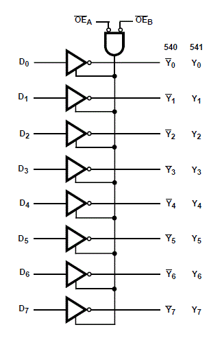
The 3-state outputs are controlled by a two-input NOR gate. If either output-enable (OE1orOE2) input is high, all eight outputs are in the high-impedance state. The SNx4HC541 devices provide true data at the outputs.


