Catalog
9-Bit Bus Transceivers With 3-State Outputs
Key Features
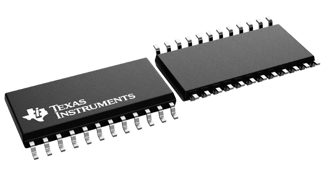
• State-of-the-ArtEPIC-IIBTMBiCMOS Design Significantly Reduces Power DissipationTypical VOLP(Output Ground Bounce) < 1 V at VCC= 5 V, TA= 25°CHigh-Impedance State During Power Up and Power DownHigh-Drive Outputs (-32-mA IOH, 64-mA IOL)Latch-Up Performance Exceeds 500 mA Per JESD 17ESD Protection Exceeds 2000 V Per MIL-STD-883, Method 3015; Exceeds 200 V Using Machine Model (C = 200 pF, R = 0)Package Options Include Plastic Small-Outline (DW), Shrink Small-Outline (DB) Packages, and Thin Shrink Small-Outline (PW), Ceramic Chip Carriers (FK), Plastic (NT), and Ceramic (JT) DIPsEPIC-IIB is a trademark of Texas Instruments Incorporated.State-of-the-ArtEPIC-IIBTMBiCMOS Design Significantly Reduces Power DissipationTypical VOLP(Output Ground Bounce) < 1 V at VCC= 5 V, TA= 25°CHigh-Impedance State During Power Up and Power DownHigh-Drive Outputs (-32-mA IOH, 64-mA IOL)Latch-Up Performance Exceeds 500 mA Per JESD 17ESD Protection Exceeds 2000 V Per MIL-STD-883, Method 3015; Exceeds 200 V Using Machine Model (C = 200 pF, R = 0)Package Options Include Plastic Small-Outline (DW), Shrink Small-Outline (DB) Packages, and Thin Shrink Small-Outline (PW), Ceramic Chip Carriers (FK), Plastic (NT), and Ceramic (JT) DIPsEPIC-IIB is a trademark of Texas Instruments Incorporated.
Description
AI
The 'ABT863 devices are 9-bit transceivers designed for asynchronous communication between data buses. The control-function implementation allows for maximum flexibility in timing.
These devices allow noninverted data transmission from the A bus to the B bus or from the B bus to the A bus, depending on the logic levels at the output-enable (OEAB\ and OEBA\) inputs.
The outputs are in the high-impedance state during power up and power down. The outputs remain in the high-impedance state while the device is powered down.
When VCCis between 0 and 2.1 V, the device is in the high-impedance state during power up or power down. However, to ensure the high-impedance state above 2.1 V, OE\ should be tied to VCCthrough a pullup resistor; the minimum value of the resistor is determined by the current-sinking capability of the driver.
The SN54ABT863 is characterized for operation over the full military temperature range of -55°C to 125°C.The SN74ABT863 is characterized for operation from -40°C to 85°C.


