Catalog
2-channel output LVCMOS 1.8-V buffer
Key Features
• High-performance 1:2, 1:3 or 1:4 LVCMOS clock bufferVery low output skew < 50 psExtremely low additive jitter < 50 fs maximum7.5 fs typical at VDD= 3.3 V10 fs typical at VDD= 2.5 V19.2 fs typical at VDD= 1.8 VVery low propagation delay < 3 nsSynchronous output enableSupply voltage: 3.3 V, 2.5 V, or 1.8 V3.3-V tolerant input at all supply voltagesFail-safe inputsfmax= 250 MHz for 3.3 V fmax= 200 MHz for 2.5 V and 1.8 VOperating temperature range: –40°C to 125°CAvailable in 8-pin TSSOP packageAvailable in 8-pin WSON packageHigh-performance 1:2, 1:3 or 1:4 LVCMOS clock bufferVery low output skew < 50 psExtremely low additive jitter < 50 fs maximum7.5 fs typical at VDD= 3.3 V10 fs typical at VDD= 2.5 V19.2 fs typical at VDD= 1.8 VVery low propagation delay < 3 nsSynchronous output enableSupply voltage: 3.3 V, 2.5 V, or 1.8 V3.3-V tolerant input at all supply voltagesFail-safe inputsfmax= 250 MHz for 3.3 V fmax= 200 MHz for 2.5 V and 1.8 VOperating temperature range: –40°C to 125°CAvailable in 8-pin TSSOP packageAvailable in 8-pin WSON package
Description
AI
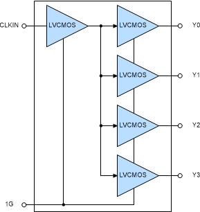
The LMK1C110x is a modular, high-performance, low-skew, general-purpose clock buffer family from Texas Instruments. The entire family is designed with a modular approach in mind. Three different fan-out variations, 1:2, 1:3, 1:4, are available.
All of the devices within this family are pin-compatible to each other and backwards compatible to the CDCLVC110x family for easy handling.
All family members share the same high performing characteristics such as low additive jitter, low skew, and wide operating temperature range.
The LMK1C110x supports a synchronous output enable control (1G) which switches the outputs into a low state when 1G is low. These devices have a fail-safe input that prevents oscillation at the outputs in the absence of an input signal and allows for input signals before VDD is supplied.
The LMK1C110x family operates in a 1.8-V, 2.5-V and 3.3-V environment and are characterized for operation from –40°C to 125°C.


