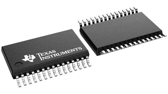
ADS7950-Q1 Series
12 bit, 1 MSPS, 4 ch, single ended, micro power, sr i/f, SAR ADC
Manufacturer: Texas Instruments
Catalog
12 bit, 1 MSPS, 4 ch, single ended, micro power, sr i/f, SAR ADC
Key Features
• Qualified for Automotive ApplicationsAEC-Q100 Tested with the Following Results:Device Temperature Grade 1: –40°C to 125°CAmbient Operating Temperature RangeDevice HBM ESD Classification Level H2Device CDM ESD Classification Level C4BProduct Family:8-, 10-, and 12-Bit Resolution4-, 8-, 12-Channel Devices Share 16 Channel Footprint1-MHz Sample-Rate Serial DevicesAnalog Supply Range: 2.7 V to 5.25 VI/O Supply Range: 1.7 V to 5.25 VTwo SW-Selectable Unipolar, Input Ranges:(0 V to 2.5 V) or (0 V to 5 V)Auto and Manual Modes for Channel SelectionTwo Programmable Alarm Levels per ChannelFour Individually Configurable GPIOsTypical Power Dissipation: 14.5 mW (V(+VA)= 5 V,V(+VBD)= 3 V) at 1 MSPSPower-Down Current (1 μA)30-Pin and 38-Pin TSSOP PackageQualified for Automotive ApplicationsAEC-Q100 Tested with the Following Results:Device Temperature Grade 1: –40°C to 125°CAmbient Operating Temperature RangeDevice HBM ESD Classification Level H2Device CDM ESD Classification Level C4BProduct Family:8-, 10-, and 12-Bit Resolution4-, 8-, 12-Channel Devices Share 16 Channel Footprint1-MHz Sample-Rate Serial DevicesAnalog Supply Range: 2.7 V to 5.25 VI/O Supply Range: 1.7 V to 5.25 VTwo SW-Selectable Unipolar, Input Ranges:(0 V to 2.5 V) or (0 V to 5 V)Auto and Manual Modes for Channel SelectionTwo Programmable Alarm Levels per ChannelFour Individually Configurable GPIOsTypical Power Dissipation: 14.5 mW (V(+VA)= 5 V,V(+VBD)= 3 V) at 1 MSPSPower-Down Current (1 μA)30-Pin and 38-Pin TSSOP Package
Description
AI
The ADS79xx is a 12-, 10-, 8-bit pin compatible multichannel analog-to-digital converter family. The device comparison table shows all twelve devices from this product family.
The devices include a capacitor based SAR A/D converter with inherent sample and hold.
The devices accept a wide analog supply range from 2.7 V to 5.25 V. Very low power consumption makes these devices suitable for battery-powered and isolated power-supply applications.
A wide 1.7-V to 5.25-V I/O supply range facilitates a glueless interface with the most commonly used digital hosts. The serial interface is controlled byCSand SCLK for easy connection with microprocessors and DSP.
The input signal is sampled with the falling edge ofCS. It uses SCLK for conversion, serial data output, and reading serial data in. The devices allow auto sequencing of preselected channels or manual selection of a channel for the next conversion cycle.
There are two software selectable input ranges (0 V to VREFand 0 V to 2 × VREF), individually configurable GPIOs (four in case of the TSSOP and one on the VQFN package devices), and two programmable alarm thresholds per channel. These features make the devices suitable for most data acquisition applications.
The devices offer an attractive power-down feature. This is extremely useful for power saving when the device is operated at lower conversion speeds.
The 16-, 12-channel devices from this family are available in a 38-pin TSSOP and 32 pin VQFN package and the 4/8-channel devices are available in a 30-pin TSSOP and 24 pin VQFN packages.


