THS1206-EP Series
12-Bit, 6 MSPS ADC Quad Ch. (Config.), DSP/uP IF, Integ. 16x FIFO, Channel AutoScan, Low Power
Manufacturer: Texas Instruments
Catalog
12-Bit, 6 MSPS ADC Quad Ch. (Config.), DSP/uP IF, Integ. 16x FIFO, Channel AutoScan, Low Power
Key Features
• Controlled BaselineOne Assembly/Test Site, One Fabrication SiteExtended Temperature Performance of –55°C to 125°CEnhanced Diminishing Manufacturing Sources (DMS) SupportEnhanced Product Change NotificationQualification PedigreeHigh-Speed 6 MSPS ADC4 Single-Ended or 2 Differential InputsSimultaneous Sampling of 4 Single-Ended Signals or 2 Differential Signals or Combination of BothDifferential Nonlinearity Error: ±1 LSBIntegral Nonlinearity Error: ±1.8 LSBSignal-to-Noise and Distortion Ratio: 68 dB at fI= 2 MHzAuto-Scan Mode for 2, 3, or 4 Inputs3-V or 5-V Digital Interface CompatibleLow Power: 216 mW Max5-V Analog Single Supply OperationInternal Voltage References . . . 50 PPM/°C and ±5% AccuracyGlueless DSP InterfaceParallel µC/DSP InterfaceIntegrated FIFOAvailable in TSSOP PackageapplicationsRadar ApplicationsCommunicationsControl ApplicationsHigh-Speed DSP Front-EndSelected Military ApplicationsComponent qualification in accordance with JEDEC and industry standards to ensure reliable operation over an extended temperature range. This includes, but is not limited to, Highly Accelerated Stress Test (HAST) or biased 85/85, temperature cycle, autoclave or unbiased HAST, electromigration, bond intermetallic life, and mold compound life. Such qualification testing should not be viewed as justifying use of this component beyond specified performance and environmental limits.Controlled BaselineOne Assembly/Test Site, One Fabrication SiteExtended Temperature Performance of –55°C to 125°CEnhanced Diminishing Manufacturing Sources (DMS) SupportEnhanced Product Change NotificationQualification PedigreeHigh-Speed 6 MSPS ADC4 Single-Ended or 2 Differential InputsSimultaneous Sampling of 4 Single-Ended Signals or 2 Differential Signals or Combination of BothDifferential Nonlinearity Error: ±1 LSBIntegral Nonlinearity Error: ±1.8 LSBSignal-to-Noise and Distortion Ratio: 68 dB at fI= 2 MHzAuto-Scan Mode for 2, 3, or 4 Inputs3-V or 5-V Digital Interface CompatibleLow Power: 216 mW Max5-V Analog Single Supply OperationInternal Voltage References . . . 50 PPM/°C and ±5% AccuracyGlueless DSP InterfaceParallel µC/DSP InterfaceIntegrated FIFOAvailable in TSSOP PackageapplicationsRadar ApplicationsCommunicationsControl ApplicationsHigh-Speed DSP Front-EndSelected Military ApplicationsComponent qualification in accordance with JEDEC and industry standards to ensure reliable operation over an extended temperature range. This includes, but is not limited to, Highly Accelerated Stress Test (HAST) or biased 85/85, temperature cycle, autoclave or unbiased HAST, electromigration, bond intermetallic life, and mold compound life. Such qualification testing should not be viewed as justifying use of this component beyond specified performance and environmental limits.
Description
AI
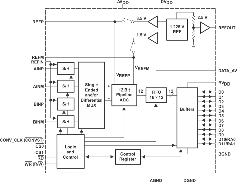
The THS1206 is a CMOS, low-power, 12-bit, 6 MSPS analog-to-digital converter (ADC). The speed, resolution, bandwidth, and single-supply operation are suited for applications in radar, imaging, high-speed acquisition, and communications. A multistage pipelined architecture with output error correction logic provides for no missing codes over the full operating temperature range. Internal control registers are used to program the ADC into the desired mode. The THS1206 consists of four analog inputs, which are sampled simultaneously. These inputs can be selected individually and configured to single-ended or differential inputs. An integrated 16 word deep FIFO allows the storage of data in order to take the load off of the processor connected to the ADC. Internal reference voltages for the ADC (1.5 V and 3.5 V) are provided.
An external reference can also be chosen to suit the dc accuracy and temperature drift requirements of the application. Two different conversion modes can be selected. In single conversion mode, a single and simultaneous conversion of up to four inputs can be initiated by using the single conversion start signal (CONVST)\. The conversion clock in single conversion mode is generated internally using a clock oscillator circuit. In continuous conversion mode, an external clock signal is applied to the CONV_CLK input of the THS1206. The internal clock oscillator is switched off in continuous conversion mode.
The THS1206C is characterized for operation from 0°C to 70°C, the THS1206I is characterized for operation from –40°C to 85°C, the THS1206Q is characterized to meet the rigorous requirements of the automotive environment from –40°C to 125°C, and the THS1206M is characterized for operation over the full military temperature range of –55°C to 125°C.


