SN74LVC1G00-EP Series
Enhanced product single 1-input, 1.65-V to 5.5-V NAND gate
Manufacturer: Texas Instruments
Catalog
Enhanced product single 1-input, 1.65-V to 5.5-V NAND gate
Key Features
• Controlled BaselineOne Assembly/Test Site, One Fabrication SiteEnhanced Diminishing Manufacturing Sources (DMS) SupportEnhanced Product-Change NotificationQualification Pedigree(1)Supports 5-V VCCOperationInputs Accept Voltages to 5.5 VMax tpdof 3.8 ns at 3.3 VLow Power Consumption, 10-µA Max ICC±24-mA Output Drive at 3.3 VIoffSupports Partial-Power-Down Mode OperationLatch-Up Performance Exceeds 100 mA Per JESD 78, Class IIESD Protection Exceeds JESD 222000-V Human-Body Model (A114-A)200-V Machine Model (A115-A)1000-V Charged-Device Model (C101)(1)Component qualification in accordance with JEDEC and industry standards to ensure reliable operation over an extended temperature range. This includes, but is not limited to, Highly Accelerated Stress Test (HAST) or biased 85/85, temperature cycle, autoclave or unbiased HAST, electromigration, bond intermetallic life, and mold compound life. Such qualification testing should not be viewed as justifying use of this component beyond specified performance and environmental limits.Controlled BaselineOne Assembly/Test Site, One Fabrication SiteEnhanced Diminishing Manufacturing Sources (DMS) SupportEnhanced Product-Change NotificationQualification Pedigree(1)Supports 5-V VCCOperationInputs Accept Voltages to 5.5 VMax tpdof 3.8 ns at 3.3 VLow Power Consumption, 10-µA Max ICC±24-mA Output Drive at 3.3 VIoffSupports Partial-Power-Down Mode OperationLatch-Up Performance Exceeds 100 mA Per JESD 78, Class IIESD Protection Exceeds JESD 222000-V Human-Body Model (A114-A)200-V Machine Model (A115-A)1000-V Charged-Device Model (C101)(1)Component qualification in accordance with JEDEC and industry standards to ensure reliable operation over an extended temperature range. This includes, but is not limited to, Highly Accelerated Stress Test (HAST) or biased 85/85, temperature cycle, autoclave or unbiased HAST, electromigration, bond intermetallic life, and mold compound life. Such qualification testing should not be viewed as justifying use of this component beyond specified performance and environmental limits.
Description
AI
This single 2-input positive-NAND gate is designed for 1.65-V to 5.5-V VCCoperation.
The SN74LVC1G00 performs the Boolean functionY =A × Bor Y =A+Bin positive logic.
The CMOS device has high output drive while maintaining low static power dissipation over a broad VCCoperating range.
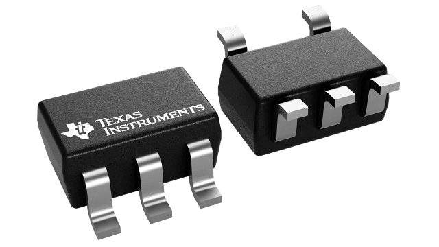
The SN74LVC1G00 is available in a variety of packages, including the ultra-small DPW package with a body size of 0.8 mm × 0.8 mm.


