Catalog
6-ch, 3-V to 18-V buffers
Key Features
• 1 TTL-load output drive capability2 output-disable controls3-state outputsPin compatible with industry types MM80C97, MC14503, and 3400975-V, 10-V, and 15-V parametric ratingsMaximum input current of 1 µA at 18 V over full package-temperature range; 100 nA at 18 V and 25°CMeets all requirements of JEDEC Tentative Standard No. 13B, "Standard Specifications for Description of 'B' Series CMOS Devices"1 TTL-load output drive capability2 output-disable controls3-state outputsPin compatible with industry types MM80C97, MC14503, and 3400975-V, 10-V, and 15-V parametric ratingsMaximum input current of 1 µA at 18 V over full package-temperature range; 100 nA at 18 V and 25°CMeets all requirements of JEDEC Tentative Standard No. 13B, "Standard Specifications for Description of 'B' Series CMOS Devices"
Description
AI
CD4502B is a hex noninverting buffer with 3-state outputs having high sink- and source-current capability. Two disable controls are provided, one of which controls four buffers and the other controls the remaining two buffers.
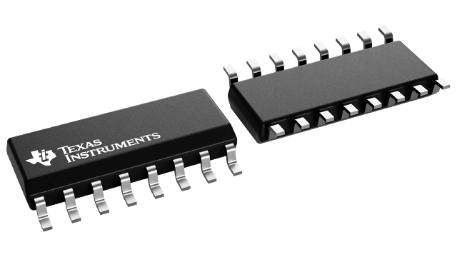
The CD4503B types are supplied in 16-lead hermetic dual-in-line ceramic packages (F3A suffix), 16-lead dual-in-line plastic packages (E suffix), 16-lead small-outline packages (M, M96, MT and NSR suffixes), and 16-lead thin shrink small-outline packages (PW and PWR suffixes).


