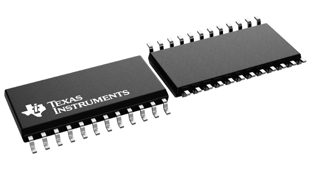
SN74ALS646A Series
Octal Registered Bus Transceivers with 3-State Outputs
Manufacturer: Texas Instruments
Catalog
Octal Registered Bus Transceivers with 3-State Outputs
Key Features
• Independent Registers for A and B BusesMultiplexed Real-Time and Stored DataChoice of True or Inverting Data PathsChoice of 3-State or Open-Collector OutputsPackage Options Include Plastic Small-Outline (DW) Packages, Ceramic Chip Carriers (FK), and Standard Plastic (NT) and Ceramic (JT) 300-mil DIPsIndependent Registers for A and B BusesMultiplexed Real-Time and Stored DataChoice of True or Inverting Data PathsChoice of 3-State or Open-Collector OutputsPackage Options Include Plastic Small-Outline (DW) Packages, Ceramic Chip Carriers (FK), and Standard Plastic (NT) and Ceramic (JT) 300-mil DIPs
Description
AI
These devices consist of bus-transceiver circuits with 3-state or open-collector outputs, D-type flip-flops, and control circuitry arranged for multiplexed transmission of data directly from the data bus or from the internal storage registers. Data on the A or B bus is clocked into the registers on the low-to-high transition of the appropriate clock (CLKAB or CLKBA) input. Figure 1 illustrates the four fundamental bus-management functions that can be performed with the octal bus transceivers and registers.
Output-enable () and direction-control (DIR) inputs control the transceiver functions. In the transceiver mode, data present at the high-impedance port may be stored in either or both registers.
The select-control (SAB and SBA) inputs can multiplex stored and real-time (transparent mode)
data. The circuitry used for select control eliminates the typical decoding glitch that occurs in a multiplexer during the transition between stored and real-time data. DIR determines which bus receives data whenis low. In the isolation mode (high), A data may be stored in one register and/or B data may be stored in the other register.
When an output function is disabled, the input function is still enabled and can be used to store and transmit data. Only one of the two buses, A or B, may be driven at a time.
The -1 version of the SN74ALS646A is identical to the standard version, except that the recommended maximum IOLin the -1 version is increased to 48 mA. There are no -1 versions of the SN54ALS646, SN54ALS648, or SN74ALS648A.
The SN54ALS646, SN54ALS648, and SN54AS646 are characterized for operation over the full military temperature range of -55°C to 125°C. The SN74ALS646A, SN74ALS648A, SN74AS646, and SN74AS648 are characterized for operation from 0°C to 70°C.


