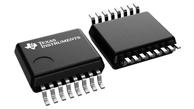
MAX3221-EP Series
3- to 5.5-V single channel 250kbps RS-232 line driver/receiver with +/-15-kV IEC-ESD protection
Manufacturer: Texas Instruments
Catalog
3- to 5.5-V single channel 250kbps RS-232 line driver/receiver with +/-15-kV IEC-ESD protection
Key Features
• Controlled BaselineOne Assembly/Test Site, One Fabrication SiteExtended Temperature Performance of -55°C to 125°CEnhanced Diminishing Manufacturing Sources (DMS) SupportEnhanced Product-Change NotificationQualification Pedigree(1)RS-232 Bus-Pin ESD Protection Exceeds ±15 kV Using Human-Body Model (HBM)Meets or Exceeds the Requirements of TIA/EIA-232-F and ITU v.28 StandardsOperates With 3-V to 5.5-V VCCSupplyOperates up to 250 kbit/sOne Driver and One ReceiverLow Standby Current . . . 1 µA TypicalExternal Capacitors . . . 4 × 0.1 µFAccepts 5-V Logic Input With 3.3-V SupplyAlternative High-Speed Pin-Compatible Device (1 Mbit/s)SNx5C3221Auto-Powerdown Feature Automatically Disables Drivers for Power SavingsAPPLICATIONSBattery-Powered, Hand-Held, and Portable EquipmentPDAs and Palmtop PCsNotebooks, Subnotebooks, and LaptopsDigital CamerasMobile Phones and Wireless Devices(1)Component qualification in accordance with JEDEC and industry standards to ensure reliable operation over an extended temperature range. This includes, but is not limited to, Highly Accelerated Stress Test (HAST) or biased 85/85, temperature cycle, autoclave or unbiased HAST, electromigration, bond intermetallic life, and mold compound life. Such qualification testing should not be viewed as justifying use of this component beyond specified performance and environmental limits.Controlled BaselineOne Assembly/Test Site, One Fabrication SiteExtended Temperature Performance of -55°C to 125°CEnhanced Diminishing Manufacturing Sources (DMS) SupportEnhanced Product-Change NotificationQualification Pedigree(1)RS-232 Bus-Pin ESD Protection Exceeds ±15 kV Using Human-Body Model (HBM)Meets or Exceeds the Requirements of TIA/EIA-232-F and ITU v.28 StandardsOperates With 3-V to 5.5-V VCCSupplyOperates up to 250 kbit/sOne Driver and One ReceiverLow Standby Current . . . 1 µA TypicalExternal Capacitors . . . 4 × 0.1 µFAccepts 5-V Logic Input With 3.3-V SupplyAlternative High-Speed Pin-Compatible Device (1 Mbit/s)SNx5C3221Auto-Powerdown Feature Automatically Disables Drivers for Power SavingsAPPLICATIONSBattery-Powered, Hand-Held, and Portable EquipmentPDAs and Palmtop PCsNotebooks, Subnotebooks, and LaptopsDigital CamerasMobile Phones and Wireless Devices(1)Component qualification in accordance with JEDEC and industry standards to ensure reliable operation over an extended temperature range. This includes, but is not limited to, Highly Accelerated Stress Test (HAST) or biased 85/85, temperature cycle, autoclave or unbiased HAST, electromigration, bond intermetallic life, and mold compound life. Such qualification testing should not be viewed as justifying use of this component beyond specified performance and environmental limits.
Description
AI
The MAX3221 consists of one line driver, one line receiver, and a dual charge-pump circuit with ±15-kV ESD protection pin to pin (serial-port connection pins, including GND). The device meets the requirements of TIA/EIA-232-F and provides the electrical interface between an asynchronous communication controller and the serial-port connector. The charge pump and four small external capacitors allow operation from a single 3-V to 5.5-V supply. These devices operate at data signaling rates up to 250 kbit/s and a maximum of 30-V/µs driver output slew rate.
Flexible control options for power management are available when the serial port is inactive. The auto-powerdown feature functions when FORCEON is low andFORCEOFFis high. During this mode of operation, if the device does not sense a valid RS-232 signal on the receiver input, the driver output is disabled. IfFORCEOFFis set low and enable (EN) is high, both the driver and receiver are shut off, and the supply current is reduced to 1 µA. Disconnecting the serial port or turning off the peripheral drivers causes the auto-powerdown condition to occur. Auto-powerdown can be disabled when FORCEON andFORCEOFFare high. With auto-powerdown enabled, the device is activated automatically when a valid signal is applied to the receiver input. TheINVALIDoutput notifies the user if an RS-232 signal is present at the receiver input.INVALIDis high (valid data) if the receiver input voltage is greater than 2.7 V or less than -2.7 V, or has been between -0.3 V and 0.3 V for less than 30 µs.INVALIDis low (invalid data) if the receiver input voltage is between -0.3 V and 0.3 V for more than 30 µs.


