TLC2543-EP Series
Enhanced Product 12-Bit Analog-to-Digital Converter (ADC) With Serial Control and 11 Analog Inputs
Manufacturer: Texas Instruments
Catalog
Enhanced Product 12-Bit Analog-to-Digital Converter (ADC) With Serial Control and 11 Analog Inputs
Key Features
• Controlled BaselineOne Assembly/Test Site, One Fabrication SiteExtended Temperature Performance of -40°C to 125°C (TLC2543Q) and -55°C to 125°C (TLC2543M)Enhanced Diminishing Manufacturing Sources (DMS) SupportEnhanced Product Change NotificationQualification Pedigree(1)12-Bit-Resolution Analog-to-Digital Converter (ADC)10-µs Conversion Time Over Operating Temperature11 Analog Input ChannelsThree Built-In Self-Test ModesInherent Sample-and-Hold FunctionLinearity Error . . . ±1 LSB MaxOn-Chip System ClockEnd-of-Conversion (EOC) OutputUnipolar or Bipolar Output Operation (Signed Binary With Respect to 1/2 the Applied Voltage Reference)Programmable Most Significant Bit (MSB) or Least Significant Bit (LSB) FirstProgrammable Power DownProgrammable Output Data LengthCMOS TechnologyApplication Report Available(2)(1)Component qualification in accordance with JEDEC and industry standards to ensure reliable operation over an extended temperature range. This includes, but is not limited to, Highly Accelerated Stress Test (HAST) or biased 85/85, temperature cycle, autoclave or unbiased HAST, electromigration, bond intermetallic life, and mold compound life. Such qualification testing should not be viewed as justifying use of this component beyond specified performance and environmental limits.(2)Microcontroller Based Data Acquisition Using the TLC2543 12-bit Serial-Out ADC(SLAA012)Controlled BaselineOne Assembly/Test Site, One Fabrication SiteExtended Temperature Performance of -40°C to 125°C (TLC2543Q) and -55°C to 125°C (TLC2543M)Enhanced Diminishing Manufacturing Sources (DMS) SupportEnhanced Product Change NotificationQualification Pedigree(1)12-Bit-Resolution Analog-to-Digital Converter (ADC)10-µs Conversion Time Over Operating Temperature11 Analog Input ChannelsThree Built-In Self-Test ModesInherent Sample-and-Hold FunctionLinearity Error . . . ±1 LSB MaxOn-Chip System ClockEnd-of-Conversion (EOC) OutputUnipolar or Bipolar Output Operation (Signed Binary With Respect to 1/2 the Applied Voltage Reference)Programmable Most Significant Bit (MSB) or Least Significant Bit (LSB) FirstProgrammable Power DownProgrammable Output Data LengthCMOS TechnologyApplication Report Available(2)(1)Component qualification in accordance with JEDEC and industry standards to ensure reliable operation over an extended temperature range. This includes, but is not limited to, Highly Accelerated Stress Test (HAST) or biased 85/85, temperature cycle, autoclave or unbiased HAST, electromigration, bond intermetallic life, and mold compound life. Such qualification testing should not be viewed as justifying use of this component beyond specified performance and environmental limits.(2)Microcontroller Based Data Acquisition Using the TLC2543 12-bit Serial-Out ADC(SLAA012)
Description
AI
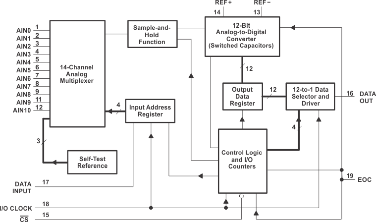
The TLC2543C and TLC2543I are 12-bit, switched-capacitor, successive-approximation, analog-to-digital converters. Each device, with three control inputs [chip select (CS\), the input-output clock, and the address input (DATA INPUT)], is designed for communication with the serial port of a host processor or peripheral through a serial 3-state output. The device allows high-speed data transfers from the host.
In addition to the high-speed converter and versatile control capability, the device has an on-chip 14-channel multiplexer that can select any one of 11 inputs or any one of three internal self-test voltages. The sample-and-hold function is automatic. At the end of conversion, the end-of-conversion (EOC) output goes high to indicate that conversion is complete. The converter incorporated in the device features differential high-impedance reference inputs that facilitate ratiometric conversion, scaling, and isolation of analog circuitry from logic and supply noise. A switched-capacitor design allows low-error conversion over the full operating temperature range.
The TLC2543C is characterized for operation from TA= 0°C to 70°C. The TLC2543I is characterized for operation from TA= –40°C to 85°C. The TLC2543M is characterized for operation from TA= –55°C to 125°C.


