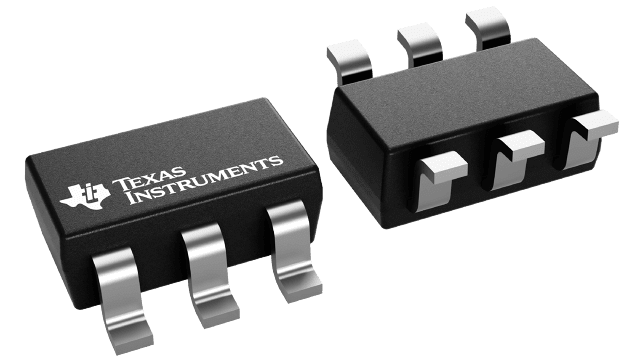
TXB0101 Series
Manufacturer: Texas Instruments

IC TRANSLTR BIDIRECTIONAL SC70-6
| Part | Operating Temperature [Max] | Operating Temperature [Min] | Channels per Circuit | Channel Type | Package / Case | Number of Circuits | Mounting Type | Output Type | Voltage - VCCA [Min] | Voltage - VCCA [Max] | Supplier Device Package | Translator Type | Data Rate | Voltage - VCCB [Min] | Voltage - VCCB [Max] | Features |
|---|---|---|---|---|---|---|---|---|---|---|---|---|---|---|---|---|
Texas Instruments | 85 C | -40 ¯C | 1 | Bidirectional | 6-TSSOP SC-88 SOT-363 | 1 | Surface Mount | Non-Inverted Tri-State | 1.2 V | 3.6 V | SC-70-6 | Voltage Level | 100 Mbps | 1.65 V | 5.5 V | Auto-Direction Sensing |
Texas Instruments | 85 C | -40 ¯C | 1 | Bidirectional | SOT-23-6 | 1 | Surface Mount | Non-Inverted Tri-State | 1.2 V | 3.6 V | SOT-23-6 | Voltage Level | 100 Mbps | 1.65 V | 5.5 V | Auto-Direction Sensing |
Texas Instruments | 85 C | -40 ¯C | 1 | Bidirectional | SOT-563 SOT-666 | 1 | Surface Mount | Non-Inverted Tri-State | 1.2 V | 3.6 V | SOT-5X3 | Voltage Level | 100 Mbps | 1.65 V | 5.5 V | Auto-Direction Sensing |
Texas Instruments | 85 C | -40 ¯C | 1 | Bidirectional | 6-TSSOP SC-88 SOT-363 | 1 | Surface Mount | Non-Inverted Tri-State | 1.2 V | 3.6 V | SC-70-6 | Voltage Level | 100 Mbps | 1.65 V | 5.5 V | Auto-Direction Sensing |
Texas Instruments | 85 C | -40 ¯C | 1 | Bidirectional | 6-TSSOP SC-88 SOT-363 | 1 | Surface Mount | Non-Inverted Tri-State | 1.2 V | 3.6 V | SC-70-6 | Voltage Level | 100 Mbps | 1.65 V | 5.5 V | Auto-Direction Sensing |
Texas Instruments | 85 C | -40 ¯C | 1 | Bidirectional | SOT-23-6 | 1 | Surface Mount | Non-Inverted Tri-State | 1.2 V | 3.6 V | SOT-23-6 | Voltage Level | 100 Mbps | 1.65 V | 5.5 V | Auto-Direction Sensing |
Texas Instruments | 85 C | -40 ¯C | 1 | Bidirectional | SOT-563 SOT-666 | 1 | Surface Mount | Non-Inverted Tri-State | 1.2 V | 3.6 V | SOT-5X3 | Voltage Level | 100 Mbps | 1.65 V | 5.5 V | Auto-Direction Sensing |
Texas Instruments | 85 C | -40 ¯C | 1 | Bidirectional | SOT-23-6 | 1 | Surface Mount | Non-Inverted Tri-State | 1.2 V | 3.6 V | SOT-23-6 | Voltage Level | 100 Mbps | 1.65 V | 5.5 V | Auto-Direction Sensing |
Texas Instruments | 85 C | -40 ¯C | 1 | Bidirectional | 6-TSSOP SC-88 SOT-363 | 1 | Surface Mount | Non-Inverted Tri-State | 1.2 V | 3.6 V | SC-70-6 | Voltage Level | 100 Mbps | 1.65 V | 5.5 V | Auto-Direction Sensing |
Texas Instruments | 85 C | -40 ¯C | 1 | Bidirectional | 6-XFBGA DSBGA | 1 | Surface Mount | Non-Inverted Tri-State | 1.2 V | 3.6 V | 6-DSBGA | Voltage Level | 100 Mbps | 1.65 V | 5.5 V | Auto-Direction Sensing |