Catalog
8-ch, 2.7-V to 3.6-V buffers with 3-state outputs
Key Features
• Operates From 2.7 V to 3.6 VInputs Accept Voltages to 5.5 VMax tpdof 5.9 ns at 3.3 VTypical VOLP(Output Ground Bounce)< 0.8 V at VCC= 3.3 V, TA= 25°CTypical VOHV(Output VOHUndershoot)> 2 V at VCC= 3.3 V, TA= 25°CIoffSupports Live Insertion, Partial-Power-Down Mode, and Back-Drive ProtectionSupports Mixed-Mode Signal Operationon All Ports (5-V Input/Output VoltageWith 3.3-V VCC)Latch-Up Performance Exceeds 100 mAPer JESD 78, Class IIOperates From 2.7 V to 3.6 VInputs Accept Voltages to 5.5 VMax tpdof 5.9 ns at 3.3 VTypical VOLP(Output Ground Bounce)< 0.8 V at VCC= 3.3 V, TA= 25°CTypical VOHV(Output VOHUndershoot)> 2 V at VCC= 3.3 V, TA= 25°CIoffSupports Live Insertion, Partial-Power-Down Mode, and Back-Drive ProtectionSupports Mixed-Mode Signal Operationon All Ports (5-V Input/Output VoltageWith 3.3-V VCC)Latch-Up Performance Exceeds 100 mAPer JESD 78, Class II
Description
AI
This octal buffer/line driver is designed for 2.7-V to 3.6-V VCCoperation.
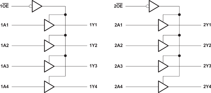
The SN74LVCZ244A device is organized as two 4-bit line drivers with separate output-enable (OE) inputs. WhenOEis low, the device passes data from the A inputs to the Y outputs. WhenOEis high, the outputs are in the high-impedance state.


