SN74LV1T125-Q1 Series
Single power supply, single buffer gate w/ 3-state output with active low enable
Manufacturer: Texas Instruments
Catalog
Single power supply, single buffer gate w/ 3-state output with active low enable
Key Features
• AEC-Q100 qualified for automotive applications:Device temperature grade 1: -40°C to +125°CDevice HBM ESD classification level 2Device CDM ESD classifcation level C4BWide operating range of 1.8 V to 5.5 VSingle-supply voltage translator (refer to LVxT Enhanced Input Voltage):Up translation:1.2 V to 1.8 V1.5 V to 2.5 V1.8 V to 3.3 V3.3 V to 5.0 VDown translation:5.0 V, 3.3 V, 2.5 V to 1.8 V5.0 V, 3.3 V to 2.5 V5.0 V to 3.3 V5.5-V tolerant input pinsSupports standard pinoutsUp to 150 Mbps with 5-V or 3.3-V V CCLatch-up performance exceeds 250 mA per JESD 17AEC-Q100 qualified for automotive applications:Device temperature grade 1: -40°C to +125°CDevice HBM ESD classification level 2Device CDM ESD classifcation level C4BWide operating range of 1.8 V to 5.5 VSingle-supply voltage translator (refer to LVxT Enhanced Input Voltage):Up translation:1.2 V to 1.8 V1.5 V to 2.5 V1.8 V to 3.3 V3.3 V to 5.0 VDown translation:5.0 V, 3.3 V, 2.5 V to 1.8 V5.0 V, 3.3 V to 2.5 V5.0 V to 3.3 V5.5-V tolerant input pinsSupports standard pinoutsUp to 150 Mbps with 5-V or 3.3-V V CCLatch-up performance exceeds 250 mA per JESD 17
Description
AI
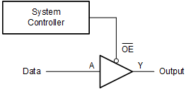
The SN74LV1T125-Q1 is a single buffer gate with 3-state outputs and integrated voltage translation. This buffer performs the Boolean function Y = A in positive logic. The outputs can be placed into a Hi-Z state by applying a High on the OE pin. The output level is referenced to the supply voltage (V CC) and supports 1.8-V, 2.5-V, 3.3-V, and 5-V CMOS levels.
The input is designed with a lower threshold circuit to support up translation for lower voltage CMOS inputs (for example, 1.2 V input to 1.8 V output or 1.8 V input to 3.3 V output). In addition, the 5-V tolerant input pins enable down translation (for example, 3.3 V to 2.5 V output).


