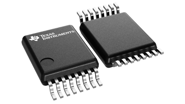
SN74CB3Q3257 Series
3.3-V, 2:1 (SPDT), 4-channel general-purpose FET bus switch
Manufacturer: Texas Instruments
Catalog
3.3-V, 2:1 (SPDT), 4-channel general-purpose FET bus switch
Key Features
• High-bandwidth data path (up to 500MHz)5V Tolerant I/Os with device powered up or powered downLow and flat on-state resistance (ron) characteristics over operating range (ron= 4Ω typical)Rail-to-rail switching on data I/O ports0- to 5V Switching with 3.3V VCC0- to 3.3V Switching with 2.5V VCCBidirectional data flow with near-zero propagation delayLow input and output capacitance minimizes loading and signal distortion (Cio(OFF) = 3.5pF typical)Fast switching frequency (f OE = 20MHz maximum)Data and control inputs provide undershoot clamp diodesLow power consumption (ICC = 0.7mA typical)VCC Operating range from 2.3V to 3.6VData I/Os support 0- to 5V signaling levels (0.8V, 1.2V, 1.5V, 1.8V, 2.5V, 3.3V, 5V)Control inputs can be driven by TTL or 5V and 3.3V CMOS outputsIoff Supports partial-power-down mode operationLatch-up performance exceeds 100mA Per JESD 78, class IIESD Performance tested per JESD 222000V Human body model (A114-B, class II)1000V Charged-device model (C101)Supports both digital and analog applications: USB interface, differential signal interface, bus isolation, low-distortion signal gating(1)(1)For additional information regarding the performance characteristics of the CB3Q family, refer to the TICBT-C, CB3T, and CB3Q Signal-Switch Familiesapplication report.High-bandwidth data path (up to 500MHz)5V Tolerant I/Os with device powered up or powered downLow and flat on-state resistance (ron) characteristics over operating range (ron= 4Ω typical)Rail-to-rail switching on data I/O ports0- to 5V Switching with 3.3V VCC0- to 3.3V Switching with 2.5V VCCBidirectional data flow with near-zero propagation delayLow input and output capacitance minimizes loading and signal distortion (Cio(OFF) = 3.5pF typical)Fast switching frequency (f OE = 20MHz maximum)Data and control inputs provide undershoot clamp diodesLow power consumption (ICC = 0.7mA typical)VCC Operating range from 2.3V to 3.6VData I/Os support 0- to 5V signaling levels (0.8V, 1.2V, 1.5V, 1.8V, 2.5V, 3.3V, 5V)Control inputs can be driven by TTL or 5V and 3.3V CMOS outputsIoff Supports partial-power-down mode operationLatch-up performance exceeds 100mA Per JESD 78, class IIESD Performance tested per JESD 222000V Human body model (A114-B, class II)1000V Charged-device model (C101)Supports both digital and analog applications: USB interface, differential signal interface, bus isolation, low-distortion signal gating(1)(1)For additional information regarding the performance characteristics of the CB3Q family, refer to the TICBT-C, CB3T, and CB3Q Signal-Switch Familiesapplication report.
Description
AI
The SN74CB3Q3257 device is a high-bandwidth FET bus switch using a charge pump to elevate the gate voltage of the pass transistor, providing a low and flat ON-state resistance (ron).
The SN74CB3Q3257 device is a high-bandwidth FET bus switch using a charge pump to elevate the gate voltage of the pass transistor, providing a low and flat ON-state resistance (ron).


