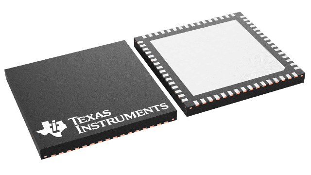
LMK04906 Series
Ultra low noise clock jitter cleaner/multiplier with 6 programmable outputs
Manufacturer: Texas Instruments
Catalog
Ultra low noise clock jitter cleaner/multiplier with 6 programmable outputs
Key Features
• Ultralow RMS Jitter Performance100-fs RMS Jitter (12 kHz to 20 MHz)123-fs RMS Jitter (100 Hz to 20 MHz)Dual Loop PLLatinum™ PLL ArchitecturePLL1Integrated Low-Noise Crystal Oscillator CircuitHoldover Mode when Input Clocks are LostAutomatic or Manual Triggering/RecoveryPLL2Normalized [1 Hz] PLL Noise Floor of –227 dBc/HzPhase Detector Rate up to 155 MHzOSCin Frequency-doublerIntegrated Low-Noise VCO3 Redundant Input Clocks with LOSAutomatic and Manual Switch-Over Modes50% Duty Cycle Output Divides, 1 to 1045 (Even and Odd)LVPECL, LVDS, or LVCMOS Programmable OutputsPrecision Digital Delay, Fixed or Dynamically Adjustable25-ps Step Analog Delay Control.6 Differential Outputs. Up to 12 Single Ended.Up to 5 VCXO/Crystal Buffered OutputsClock Rates of up to 2600 MHz0-Delay ModeThree Default Clock Outputs at Power UpMulti-mode: Dual PLL, Single PLL, and Clock DistributionIndustrial Temperature Range: –40 to 85 °C3.15-V to 3.45-V OperationPackage: 64-Pin WQFN (9 mm × 9 mm × 0.8 mm)Ultralow RMS Jitter Performance100-fs RMS Jitter (12 kHz to 20 MHz)123-fs RMS Jitter (100 Hz to 20 MHz)Dual Loop PLLatinum™ PLL ArchitecturePLL1Integrated Low-Noise Crystal Oscillator CircuitHoldover Mode when Input Clocks are LostAutomatic or Manual Triggering/RecoveryPLL2Normalized [1 Hz] PLL Noise Floor of –227 dBc/HzPhase Detector Rate up to 155 MHzOSCin Frequency-doublerIntegrated Low-Noise VCO3 Redundant Input Clocks with LOSAutomatic and Manual Switch-Over Modes50% Duty Cycle Output Divides, 1 to 1045 (Even and Odd)LVPECL, LVDS, or LVCMOS Programmable OutputsPrecision Digital Delay, Fixed or Dynamically Adjustable25-ps Step Analog Delay Control.6 Differential Outputs. Up to 12 Single Ended.Up to 5 VCXO/Crystal Buffered OutputsClock Rates of up to 2600 MHz0-Delay ModeThree Default Clock Outputs at Power UpMulti-mode: Dual PLL, Single PLL, and Clock DistributionIndustrial Temperature Range: –40 to 85 °C3.15-V to 3.45-V OperationPackage: 64-Pin WQFN (9 mm × 9 mm × 0.8 mm)
Description
AI
The LMK04906 is the industry’s highest performance clock jitter attenuator with superior clock jitter cleaning, generation, and distribution with advanced features to meet high performance timing application needs.
The LMK04906 accepts 3 clock inputs ranging from 1 kHz to 500 MHz and generates 6 unique clock output frequencies ranging from 284 kHz to 2.6 GHz. The LMK04906 can also buffer a crystal or VCXO to generate a 7thunique clock frequency.
The device provides virtually all frequency translation combinations required for SONET, Ethernet, Fibre Channel and multi-mode Wireless Base Stations.
The LMK04906 input clock frequency and clock multiplication ratio are programmable through a SPI interface.


