LMQ62440-Q1 Series
Automotive 3-V to 36-V, 4-A, low-noise fixed frequency synchronous step-down converter
Manufacturer: Texas Instruments
Catalog
Automotive 3-V to 36-V, 4-A, low-noise fixed frequency synchronous step-down converter
Key Features
• AEC-Q100 qualified for automotive applicationsTemperature grade 1: –40°C to +150°C, TJFunctional Safety-CapableDocumentation available to aid functional safety system designOptimized for ultra-low EMI requirementsMeets CISPR25 class 5 standardHotrod™ package minimizes switch node ringingInternal bypass capacitors reduce EMIParallel input path minimizes parasitic inductanceSpread spectrum reduces peak emissionsAdjustable switch node rise timeDesigned for rugged Automotive applicationsSupports 42-V load dump0.4-V dropout with 4-A load (typical)High efficiency power conversion at all loads7-µA no load current at 13.5 VIN, 3.3 VOUT90% PFM efficiency at 1-mA, 13.5 VIN, 5 VOUTLow MOSFET ON resistanceRDS_ON_HS= 41 mΩ (typical)RDS_ON_LS= 21 mΩ (typical)External bias option for improved efficiencyPin compatible with:LM62440-Q1(36 V, 4 A)AEC-Q100 qualified for automotive applicationsTemperature grade 1: –40°C to +150°C, TJFunctional Safety-CapableDocumentation available to aid functional safety system designOptimized for ultra-low EMI requirementsMeets CISPR25 class 5 standardHotrod™ package minimizes switch node ringingInternal bypass capacitors reduce EMIParallel input path minimizes parasitic inductanceSpread spectrum reduces peak emissionsAdjustable switch node rise timeDesigned for rugged Automotive applicationsSupports 42-V load dump0.4-V dropout with 4-A load (typical)High efficiency power conversion at all loads7-µA no load current at 13.5 VIN, 3.3 VOUT90% PFM efficiency at 1-mA, 13.5 VIN, 5 VOUTLow MOSFET ON resistanceRDS_ON_HS= 41 mΩ (typical)RDS_ON_LS= 21 mΩ (typical)External bias option for improved efficiencyPin compatible with:LM62440-Q1(36 V, 4 A)
Description
AI
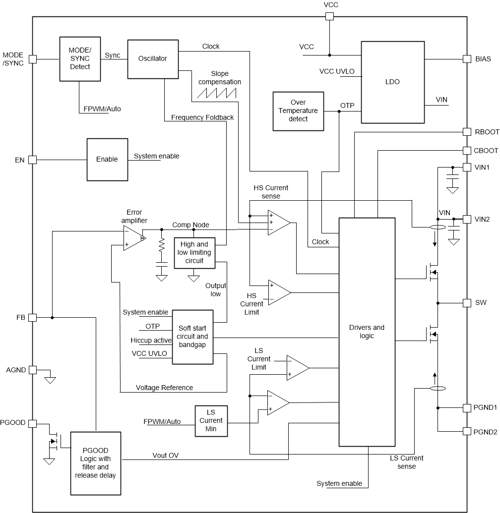
The LMQ62440-Q1 is a high-performance, DC-DC synchronous buck converter with integrated bypass capacitors. With integrated high-side and low-side MOSFETs, up to 4 A of output current is delivered over a wide input range of 3.0 V to 36 V; 42-V tolerance supports load dump for durations of 400 ms. The device implements soft recovery from dropout eliminating overshoot on the output.
The device is specifically designed for minimal EMI. The device incorporates pseudo-random spread spectrum, integrated bypass capacitors, adjustable SW node rise time, low-EMI VQFN-HR package featuring low switch node ringing, and optimized pinout for ease of use. The switching frequency can be synchronized between 200 kHz and 2.2 MHz to avoid noise sensitive frequency bands. In addition the frequency can be selected for improved efficiency at low operating frequency or smaller solution size at high operating frequency.
Auto-mode enables frequency foldback when operating at light loads, allowing an unloaded current consumption of only 7 µA (typical) and high light load efficiency. Seamless transition between PWM and PFM modes, along with very low MOSFET ON resistances and an external bias input, ensures exceptional efficiency across the entire load range.
The device is available in a 14-pin VQFN-HR package with wettable flanks. Electrical characteristics are specified over a junction temperature range of –40°C to +150°C. Find additional resources in theRelated Documentation.


