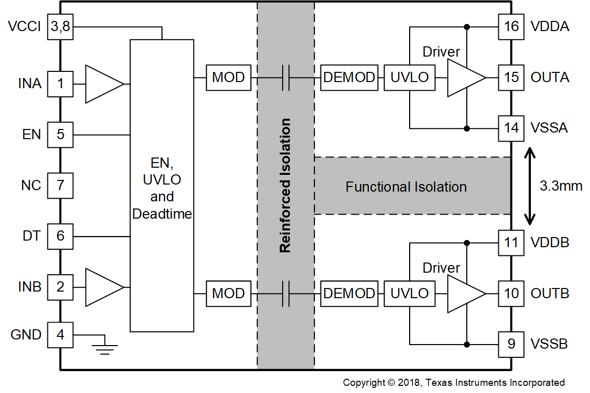
UCC21530-Q1 Series
Manufacturer: Texas Instruments

AUTOMOTIVE, 4A, 6A, 5.7KVRMS, ISOLATED DUAL-CHANNEL GATE DRIVER WITH EN AND DT PINS FOR IGBT/SIC
| Part | Approval Agency | Pulse Width Distortion (Max) [Max] | Qualification | Voltage - Output Supply [Min] | Voltage - Output Supply [Max] | Number of Channels | Voltage - Isolation | Current - Peak Output | Rise / Fall Time (Typ) [custom] | Rise / Fall Time (Typ) [custom] | Current - Output High, Low [custom] | Current - Output High, Low [custom] | Mounting Type | Operating Temperature [Min] | Operating Temperature [Max] | Grade | Propagation Delay tpLH / tpHL (Max) | Technology | Common Mode Transient Immunity (Min) [Min] | Package / Case | Package / Case [x] | Package / Case [custom] | Gate Type | Logic Voltage - VIL, VIH | Current - Peak Output (Source, Sink) [custom] | Current - Peak Output (Source, Sink) [custom] | Channel Type | Driven Configuration | Voltage - Supply [Min] | Voltage - Supply [Max] | Number of Drivers | Input Type | Propagation Delay tpLH / tpHL (Max) [Max] [custom] | Propagation Delay tpLH / tpHL (Max) [Max] [custom] |
|---|---|---|---|---|---|---|---|---|---|---|---|---|---|---|---|---|---|---|---|---|---|---|---|---|---|---|---|---|---|---|---|---|---|---|
Texas Instruments | IEC/EN/DIN UL VDE | 6 ns | AEC-Q100 | 13.5 V | 25 V | 2 | 5700 Vrms | 4 A 6 A | 7 ns | 6 ns | 6 A | 4 A | Surface Mount | -40 C | 150 °C | Automotive | 45 ns | Capacitive Coupling | 125 V/ns | 14-SOIC | 0.295 in | 7.5 mm | ||||||||||||
Texas Instruments | AEC-Q100 | 7 ns | 6 ns | Surface Mount | -40 °C | 130 °C | Automotive | 14-SOIC | 0.295 in | 7.5 mm | IGBT MOSFET (N-Channel P-Channel) N-Channel P-Channel MOSFET | 1.2 V 1.6 V | 6 A | 4 A | Independent | Half-Bridge | 3 V | 18 V | 2 | CMOS TTL | ||||||||||||||
Texas Instruments | CQC CSA UL VDE | 6 ns | AEC-Q100 | 14.7 V | 25 V | 2 | 5700 Vrms | 4 A 6 A | 7 ns | 6 ns | 6 A | 4 A | Surface Mount | -40 C | 125 °C | Automotive | Capacitive Coupling | 100 V/ns | 14-SOIC | 0.295 in | 7.5 mm | 30 ns | 30 ns | |||||||||||
Texas Instruments | AEC-Q100 | 7 ns | 6 ns | Surface Mount | -40 °C | 130 °C | Automotive | 14-SOIC | 0.295 in | 7.5 mm | IGBT MOSFET (N-Channel P-Channel) N-Channel P-Channel MOSFET | 1.2 V 1.6 V | 6 A | 4 A | Independent | Half-Bridge | 3 V | 18 V | 2 | CMOS TTL |