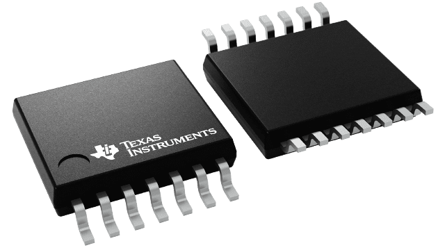
SN74LV8T164 Series
1.65-V to 5.5-V 8-bit, parallel-out serial shift registers with logic level shifter
Manufacturer: Texas Instruments
Catalog
1.65-V to 5.5-V 8-bit, parallel-out serial shift registers with logic level shifter
Key Features
• Latching logic with known power-up state provides consistent start-up behaviorWide operating range of 1.65V to 5.5V5.5V tolerant input pinsSingle-supply voltage translator (refer to LVxT Enhanced Input Voltage):Up translation:1.2V to 1.8V1.5V to 2.5V1.8V to 3.3V3.3V to 5.0VDown translation:5.0V, 3.3V, 2.5V to 1.8V5.0V, 3.3V to 2.5V5.0V to 3.3VUp to 150Mbps with 5V or 3.3V VCCSupports standard function pinoutLatch-up performance exceeds 250mAper JESD 17Latching logic with known power-up state provides consistent start-up behaviorWide operating range of 1.65V to 5.5V5.5V tolerant input pinsSingle-supply voltage translator (refer to LVxT Enhanced Input Voltage):Up translation:1.2V to 1.8V1.5V to 2.5V1.8V to 3.3V3.3V to 5.0VDown translation:5.0V, 3.3V, 2.5V to 1.8V5.0V, 3.3V to 2.5V5.0V to 3.3VUp to 150Mbps with 5V or 3.3V VCCSupports standard function pinoutLatch-up performance exceeds 250mAper JESD 17
Description
AI
The SN74LV8T164 device contains an 8-bit shift register with AND-gated serial inputs and an asynchronous clear (CLR) input. The gated serial (A and B) inputs permit complete control over incoming data; a low at either input inhibits entry of the new data and resets the first flip-flop to the low level at the next clock (CLK) pulse. A high-level input enables the other input, which then determines the state of the first flip-flop. Data at the serial inputs can be changed while CLK is high or low, provided the minimum set-up time requirements are met. Clocking occurs on the low-to-high-level transition of CLK.
The input is designed with a reduced threshold circuit to support up translation when the supply voltage is larger than the input voltage. Additionally, the 5V tolerant input pins enable down translation when the input voltage is larger than the supply voltage. The output level is always referenced to the supply voltage (VCC) and supports 1.8V, 2.5V, 3.3V, and 5V CMOS levels.


