SN65HVD379 Series
3.3 V Full-Duplex RS-485/RS-422 Drivers and Balanced Receivers
Manufacturer: Texas Instruments
Catalog
3.3 V Full-Duplex RS-485/RS-422 Drivers and Balanced Receivers
Key Features
• Designed for INTERBUS ApplicationsDesigned for RS-422 and RS-485 NetworksBalanced Receiver Thresholds1/2 Unit-Load (up to 64 nodes on the bus)Bus-Pin ESD Protection 15 kV HBMBus-Fault Protection of -7 V to 12 VThermal Shutdown ProtectionPower-Up/Down Glitch-free Bus Inputs and OutputsHigh Input Impedance With Low VCCMonotonic Outputs During Power Cycling5-V Tolerant InputsAPPLICATIONSDigital Motor ControlUtility MetersChassis-to-Chassis InterconnectionsElectronic Security StationsIndustrial, Process, and Building AutomationPoint-of-Sale (POS) Terminals and NetworksDTE/DCE InterfacesDesigned for INTERBUS ApplicationsDesigned for RS-422 and RS-485 NetworksBalanced Receiver Thresholds1/2 Unit-Load (up to 64 nodes on the bus)Bus-Pin ESD Protection 15 kV HBMBus-Fault Protection of -7 V to 12 VThermal Shutdown ProtectionPower-Up/Down Glitch-free Bus Inputs and OutputsHigh Input Impedance With Low VCCMonotonic Outputs During Power Cycling5-V Tolerant InputsAPPLICATIONSDigital Motor ControlUtility MetersChassis-to-Chassis InterconnectionsElectronic Security StationsIndustrial, Process, and Building AutomationPoint-of-Sale (POS) Terminals and NetworksDTE/DCE Interfaces
Description
AI
The SN65HVD379 is a differential line driver and differential-input line receiver that operates with a 3.3-V power supply. Each driver and receiver has separate input and output pins for full-duplex bus communication designs. They are designed for balanced transmission lines and interoperation with ANSI TIA/EIA-485A, TIA/EIA-422-B, ITU-T v.11, and ISO 8482:1993 standard-compliant devices.
These differential bus drivers and receivers are monolithic, integrated circuits designed for full-duplex bi-directional data communication on multipoint bus-transmission lines at signaling rates(1)up to 25 Mbps. The SN65HVD379 is fully enabled with no external enabling pins.
The 1/2 unit load receiver has a higher receiver input resistance. This results in lower bus leakage currents over the common-mode voltage range, and reduces the total amount of current that an RS-485 driver is forced to source or sink when transmitting.
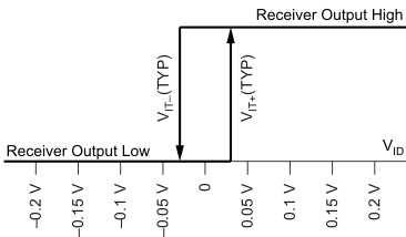
The balanced differential receiver input threshold makes the SN65HVD379 more compatible with fieldbus requirements that define an external failsafe structure.
(1)The signaling rate of a line is the number of voltage transitions that are made per second expressed in the units bps (bits per second).


