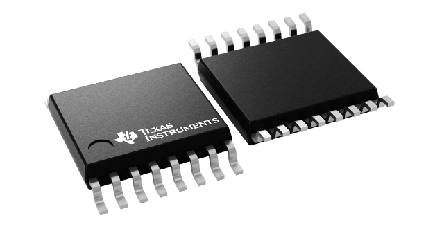
SN74LV8T594-Q1 Series
Automotive 1.65V-to-5V eight-channel shift register with logic-level shifter
Manufacturer: Texas Instruments
Catalog
Automotive 1.65V-to-5V eight-channel shift register with logic-level shifter
Key Features
• AEC-Q100 qualified for automotive applications:Device temperature grade 1: -40°C to +125°CDevice HBM ESD classification level 2Device CDM ESD classification level C4BLatching logic with known power-up state provides consistent start-up behaviorWide operating range of 1.65V to 5.5V5.5V tolerant input pinsSingle-supply voltage translator (refer to LVxT Enhanced Input Voltage):Up translation:1.2V to 1.8V1.5V to 2.5V1.8V to 3.3V3.3V to 5.0VDown translation:5.0V, 3.3V, 2.5V to 1.8V5.0V, 3.3V to 2.5V5.0V to 3.3VUp to 150Mbps with 5V or 3.3V VCCSupports standard function pinoutLatch-up performance exceeds 250mAper JESD 17AEC-Q100 qualified for automotive applications:Device temperature grade 1: -40°C to +125°CDevice HBM ESD classification level 2Device CDM ESD classification level C4BLatching logic with known power-up state provides consistent start-up behaviorWide operating range of 1.65V to 5.5V5.5V tolerant input pinsSingle-supply voltage translator (refer to LVxT Enhanced Input Voltage):Up translation:1.2V to 1.8V1.5V to 2.5V1.8V to 3.3V3.3V to 5.0VDown translation:5.0V, 3.3V, 2.5V to 1.8V5.0V, 3.3V to 2.5V5.0V to 3.3VUp to 150Mbps with 5V or 3.3V VCCSupports standard function pinoutLatch-up performance exceeds 250mAper JESD 17
Description
AI
The SN74LV8T594-Q1 device contains an 8-bit, serial-in, parallel-out shift register. Each parallel output of the shift register is fed through a storage register before reaching the primary device outputs (QA through QH). Separate clocks (SRCLK and RCLK) and direct overriding clear (SRCLR and RCLR) inputs are provided for both the shift and storage registers, allowing for loading data separately from sending it to the outputs. Additionally, the last output of the internal shift register is sent directly to the output QH’ providing a method to daisy-chain multiple shift registers.
The input is designed with a reduced threshold circuit to support up translation when the supply voltage is larger than the input voltage. Additionally, the 5V tolerant input pins enable down translation when the input voltage is larger than the supply voltage. The output level is always referenced to the supply voltage (VCC) and supports 1.8V, 2.5V, 3.3V, and 5V CMOS levels.


