SN74LV2T74-Q1 Series
Automotive 1.8-V to 5.5-V single power supply dual D-Type positive-edge-triggered flip-flops
Manufacturer: Texas Instruments
Catalog
Automotive 1.8-V to 5.5-V single power supply dual D-Type positive-edge-triggered flip-flops
Key Features
• AEC-Q100 qualified for automotive applications:Device temperature grade 1: -40°C to +125°CDevice HBM ESD classification level 2Device CDM ESD classification level C4BAvailable in wettable flank QFN (WBQA) packageWide operating range of 1.8 V to 5.5 VSingle-supply voltage translator (refer to LVxT Enhanced Input Voltage):Up translation:1.2 V to 1.8 V1.5 V to 2.5 V1.8 V to 3.3 V3.3 V to 5.0 VDown translation:5.0 V, 3.3 V, 2.5 V to 1.8 V5.0 V, 3.3 V to 2.5 V5.0 V to 3.3 V5.5-V tolerant input pinsSupports standard pinoutsUp to 150 Mbps with 5-V or 3.3-V V CCLatch-up performance exceeds 250 mA per JESD 17AEC-Q100 qualified for automotive applications:Device temperature grade 1: -40°C to +125°CDevice HBM ESD classification level 2Device CDM ESD classification level C4BAvailable in wettable flank QFN (WBQA) packageWide operating range of 1.8 V to 5.5 VSingle-supply voltage translator (refer to LVxT Enhanced Input Voltage):Up translation:1.2 V to 1.8 V1.5 V to 2.5 V1.8 V to 3.3 V3.3 V to 5.0 VDown translation:5.0 V, 3.3 V, 2.5 V to 1.8 V5.0 V, 3.3 V to 2.5 V5.0 V to 3.3 V5.5-V tolerant input pinsSupports standard pinoutsUp to 150 Mbps with 5-V or 3.3-V V CCLatch-up performance exceeds 250 mA per JESD 17
Description
AI
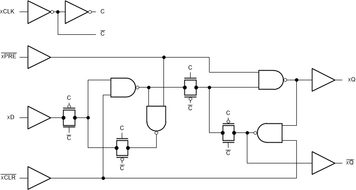
The SN74LV2T74-Q1 contains two independent D-type positive-edge-triggered flip-flops. A low level at the preset ( PRE) input sets the output high. A low level at the clear ( CLR) input resets the output low. Preset and clear functions are asynchronous and not dependent on the levels of the other inputs. When PRE and CLR are inactive (high), data at the data (D) input meeting the setup time requirements is transferred to the outputs (Q, Q) on the positive-going edge of the clock (CLK) pulse. Clock triggering occurs at a voltage level and is not directly related to the rise time of the input clock (CLK) signal. Following the hold-time interval, data at the data (D) input can be changed without affecting the levels at the outputs (Q, Q). The output level is referenced to the supply voltage (V CC) and supports 1.8-V, 2.5-V, 3.3-V, and 5-V CMOS levels.
The input is designed with a lower threshold circuit to support up translation for lower voltage CMOS inputs (for example, 1.2 V input to 1.8 V output or 1.8 V input to 3.3 V output). In addition, the 5-V tolerant input pins enable down translation (for example, 3.3 V to 2.5 V output).


