Catalog
25µA quiescent current synchronous boost converter
Key Features
• AEC-Q100 qualified for automotive applicationsDevice temperature grade 1: –40°C to 125°C ambient operating temperature rangeFunction Safety-CapableDocumentation available to aid functional safety system designFlexible input and output operation rangeInput voltage range: 2.3 V to 14 VProgrammable output voltage range: 4.0 V to 18.5 V5-V, 5.25-V, 5.5-V fixed output optionsFixed 2-A peak current limitAvoid AM band interference and crosstalkDynamically programmable switching frequency: 200 kHz to 2.2 MHzSpread spectrum frequency modulationOptional clock synchronizationMinimize solution size for space constraint applicationsIntegrated LS/HS/ISO FET: RDS(ON)50 mΩ/50 mΩ/100 mΩSupport up to 2.2 MHz with small L-CMinimized light load and idle state current consumption25-µA quiescent current into VIN pin0.5-µA shutdown current into VIN pinSelectable auto PFM and forced PWM modeTrue load disconnect during shutdown or fault conditionsIntegrated protection featuresSupport VIN close to VOUT operationInput undervoltage lockout and output overvoltage protectionHiccup output short circuit protectionPower good indicatorThermal shutdown protection at 165°CHigher than 90% efficiency under 0.25-A load from 3.3-V to 9-V conversionAEC-Q100 qualified for automotive applicationsDevice temperature grade 1: –40°C to 125°C ambient operating temperature rangeFunction Safety-CapableDocumentation available to aid functional safety system designFlexible input and output operation rangeInput voltage range: 2.3 V to 14 VProgrammable output voltage range: 4.0 V to 18.5 V5-V, 5.25-V, 5.5-V fixed output optionsFixed 2-A peak current limitAvoid AM band interference and crosstalkDynamically programmable switching frequency: 200 kHz to 2.2 MHzSpread spectrum frequency modulationOptional clock synchronizationMinimize solution size for space constraint applicationsIntegrated LS/HS/ISO FET: RDS(ON)50 mΩ/50 mΩ/100 mΩSupport up to 2.2 MHz with small L-CMinimized light load and idle state current consumption25-µA quiescent current into VIN pin0.5-µA shutdown current into VIN pinSelectable auto PFM and forced PWM modeTrue load disconnect during shutdown or fault conditionsIntegrated protection featuresSupport VIN close to VOUT operationInput undervoltage lockout and output overvoltage protectionHiccup output short circuit protectionPower good indicatorThermal shutdown protection at 165°CHigher than 90% efficiency under 0.25-A load from 3.3-V to 9-V conversion
Description
AI
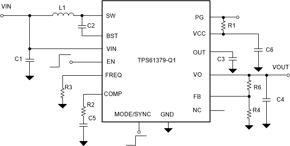
The TPS61379-Q1 is a fully integrated synchronous boost converter with load disconnect function integrated. The input voltage covers 2.3 V to 14 V, while the maximal output voltage is up to 18.5 V. The switching current limit is 2 A typical. It consumes 25-µA quiescent current from VIN.
The TPS61379-Q1 employs the peak current mode control with the switching frequency programmable from 200 kHz to 2.2 MHz. The device works in fixed frequency PWM operation in medium to heavy load. There are two optional modes in light load by configuring the MODE pin: auto PFM mode and forced PWM to balance the efficiency and noise immunity in light load. The switching frequency can be synchronized to an external clock. The TPS61379-Q1 uses the spread spectrum of the internal clock to be more EMI friendly at FPWM mode. In addition, there is an internal soft-start time to limit the inrush current.
The TPS61379-Q1 has various fixed output voltage versions to save the external feedback resistor. It supports the external loop compensation so that the stability and transient response can be optimized at wider VOUT/VINranges. It also integrates robust protection features including the output short protection, output overvoltage protection, and thermal shutdown protection. The TPS61379-Q1 is available in a 3-mm × 3-mm 16-pin QFN package with wettable flank.