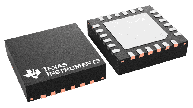
ADS8924B Series
16-bit, 250-kSPS, one-channel SAR ADC with internal VREF buffer, internal LDO and enhanced SPI
Manufacturer: Texas Instruments
Catalog
16-bit, 250-kSPS, one-channel SAR ADC with internal VREF buffer, internal LDO and enhanced SPI
Key Features
• Resolution: 16-BitsHigh Sample Rate With No Latency Output:ADS8920B: 1-MSPSADS8922B: 500-kSPSADS8924B: 250-kSPSIntegrated LDO Enables Single-Supply OperationLow Power Reference Buffer with No DroopExcellent AC and DC Performance:SNR: 96.8-dB, THD: –125-dBINL: ±0.25-LSBDNL: ±0.2-LSB, 16-Bit No-Missing-CodesWide Input Range:Unipolar Differential Input Range: ±VREFVREFInput Range: 2.5-V to 5-VSingle-Supply, Low-Power OperationEnhanced-SPI Digital InterfaceInterface SCLK: 18-MHz at 1-MSPSConfigurable Data Parity OutputExtended Temperature Range: –40°C to +125°CSmall Footprint: 4-mm × 4-mm VQFNResolution: 16-BitsHigh Sample Rate With No Latency Output:ADS8920B: 1-MSPSADS8922B: 500-kSPSADS8924B: 250-kSPSIntegrated LDO Enables Single-Supply OperationLow Power Reference Buffer with No DroopExcellent AC and DC Performance:SNR: 96.8-dB, THD: –125-dBINL: ±0.25-LSBDNL: ±0.2-LSB, 16-Bit No-Missing-CodesWide Input Range:Unipolar Differential Input Range: ±VREFVREFInput Range: 2.5-V to 5-VSingle-Supply, Low-Power OperationEnhanced-SPI Digital InterfaceInterface SCLK: 18-MHz at 1-MSPSConfigurable Data Parity OutputExtended Temperature Range: –40°C to +125°CSmall Footprint: 4-mm × 4-mm VQFN
Description
AI
The ADS8920B, ADS8922B, and ADS8924B (ADS892xB) belong to a family of pin-to-pin compatible, high-speed, single-channel, high-precision, 16-bit successive approximation register (SAR) based analog-to-digital convertors (ADCs) with an integrated reference buffer and integrated low-dropout regulator (LDO). The device family includes the ADS890xB (20-bit) and ADS891xB (18-bit) resolution variants.
The ADS89xxB boost analog performance while maintaining high-resolution data transfer by using TI’s Enhanced-SPI feature. Enhanced-SPI enables the ADS89xxB to achieve high throughput at lower clock speeds, thereby simplifying the board layout and lowering system cost. Enhanced-SPI also simplifies clocking-in of data, thereby making this device ideal for applications involving FPGAs, DSPs. The ADS89xxB is compatible with a standard SPI Interface.
The ADS89xxB has an internal data parity feature that can be appended to the ADC data output. ADC data validation by the host, using parity bits, improves system reliability.


