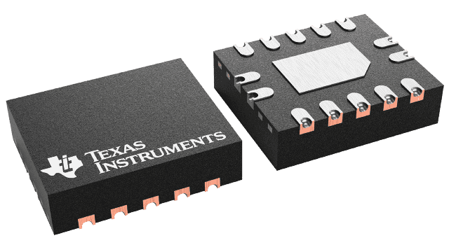
SN74LV6T07-Q1 Series
Automotive 1.8-V to 5.5-V single power supply 6-bit buffers with tri-state outputs
Manufacturer: Texas Instruments
Catalog
Automotive 1.8-V to 5.5-V single power supply 6-bit buffers with tri-state outputs
Key Features
• AEC-Q100 qualified for automotive applications:Device temperature grade 1: -40°C to +125°CDevice HBM ESD classification level 2Device CDM ESD classification level C4BAvailable in wettable flank QFN packageWide operating range of 1.65 V to 5.5 V5.5-V tolerant input pinsLVxT enhanced inputs combined with open-drain outputs provide maximum voltage translation flexibility:Over 6.67-Mbps operation, (R PU = 1 kΩ, C L = 30 pF)Up translation from 1.2 V to 5 V with 1.8-V supplyDown translation from 5 V to 0.8 V or even less with any valid supply5.5-V tolerant input pinsSupports standard function pinoutLatch-up performance exceeds 250 mA per JESD 17AEC-Q100 qualified for automotive applications:Device temperature grade 1: -40°C to +125°CDevice HBM ESD classification level 2Device CDM ESD classification level C4BAvailable in wettable flank QFN packageWide operating range of 1.65 V to 5.5 V5.5-V tolerant input pinsLVxT enhanced inputs combined with open-drain outputs provide maximum voltage translation flexibility:Over 6.67-Mbps operation, (R PU = 1 kΩ, C L = 30 pF)Up translation from 1.2 V to 5 V with 1.8-V supplyDown translation from 5 V to 0.8 V or even less with any valid supply5.5-V tolerant input pinsSupports standard function pinoutLatch-up performance exceeds 250 mA per JESD 17
Description
AI
The SN74LV6T07-Q1 device contains six independent buffers with open-drain outputs. Each buffer performs the Boolean function Y = A in positive logic.
The input is designed with a lower threshold circuit to support up translation for lower voltage CMOS inputs (for example, 1.2 V input to 1.8 V output or 1.8 V input to 3.3 V output). In addition, the 5-V tolerant input pins enable down translation (for example, 3.3 V to 2.5 V output).


