Catalog
2.35V-5.25V, 8 Bit, 1.25MSPS, Serial ADC
Key Features
• 1.25-MHz Sample Rate Serial Device10-Bit Resolution (ADS7887)8-Bit Resolution (ADS7888)Zero Latency25-MHz Serial InterfaceSupply Range: 2.35 V to 5.25 VTypical Power Dissipation at 1.25 MSPS:3.8 mW at 3-V VDD8 mw at 5-V VDD±0.35 LSB INL, DNL (ADS7887)±0.15 LSB INL, ±0.1 LSB DNL (ADS7888)61 dB SINAD, –84 dB THD (ADS7887)49.5 dB SINAD, –67.5 dB THD (ADS7888)Unipolar Input Range: 0 V to VDDPower-Down Current: 1 µAWide Input Bandwidth: 15 MHz at 3 dB6-Pin SOT23 and SC70 PackagesAll trademarks are the property of their respective owners.1.25-MHz Sample Rate Serial Device10-Bit Resolution (ADS7887)8-Bit Resolution (ADS7888)Zero Latency25-MHz Serial InterfaceSupply Range: 2.35 V to 5.25 VTypical Power Dissipation at 1.25 MSPS:3.8 mW at 3-V VDD8 mw at 5-V VDD±0.35 LSB INL, DNL (ADS7887)±0.15 LSB INL, ±0.1 LSB DNL (ADS7888)61 dB SINAD, –84 dB THD (ADS7887)49.5 dB SINAD, –67.5 dB THD (ADS7888)Unipolar Input Range: 0 V to VDDPower-Down Current: 1 µAWide Input Bandwidth: 15 MHz at 3 dB6-Pin SOT23 and SC70 PackagesAll trademarks are the property of their respective owners.
Description
AI
The ADS7887 device is a 10-bit, 1.25-MSPS, analog-to-digital converter (ADC), and the ADS7888 device is a 8-bit, 1.25-MSPS ADC. These devices include a capacitor-based SAR A/D converter with inherent sample and hold. The serial interface in each device is controlled by theCSand SCLK signals for glueless connections with microprocessors and DSPs. The input signal is sampled with the falling edge ofCS, and SCLK is used for conversion and serial data output.
The devices operate from a wide supply range from 2.35 V to 5.25 V. The low power consumption of the devices make them suitable for battery-powered applications. The devices also include a power-saving, power-down feature for when the devices are operated at lower conversion speeds.
The high level of the digital input to the device is not limited to device VDD. This means the digital input can go as high as 5.25 V when device supply is 2.35 V. This feature is useful when digital signals are coming from other circuit with different supply levels. Also this relaxes restriction on power-up sequencing.
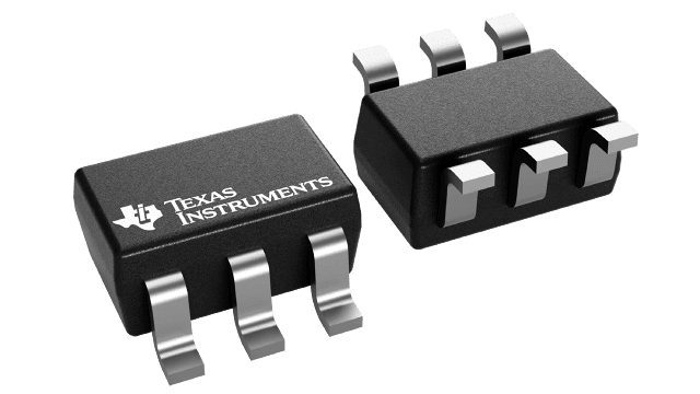
The ADS7887 and ADS7888 are available in 6-pin SOT-23 and SC70 packages and are specified for operation from –40°C to 125°C.


