Zenode.ai Logo
Beta
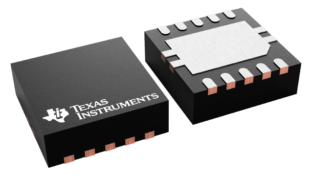
UCC27282-Q1

UCC27282-Q1 Series

Automotive 3-A, 120-V half bridge driver with 5-V UVLO, interlock and enable

Manufacturer: Texas Instruments

Catalog

Automotive 3-A, 120-V half bridge driver with 5-V UVLO, interlock and enable

PartNumber of DriversSupplier Device PackageInput TypeOperating Temperature [Max]Operating Temperature [Min]Channel TypeDriven ConfigurationPackage / CaseVoltage - Supply [Max]Voltage - Supply [Min]Rise / Fall Time (Typ) [custom]Rise / Fall Time (Typ) [custom]QualificationMounting TypeGate TypeGradeLogic Voltage - VIL, VIH [custom]Logic Voltage - VIL, VIH [custom]Current - Peak Output (Source, Sink) [custom]Current - Peak Output (Source, Sink) [custom]High Side Voltage - Max (Bootstrap) [Max]Package / Case [y]Package / Case [x]FunctionTypeUtilized IC / PartSupplied ContentsSecondary AttributesLogic Voltage - VIL, VIH
10-VSON
Texas Instruments
2
10-VSON (3x3)
Non-Inverting
125 °C
-40 °C
Independent
Half-Bridge
10-VFDFN Exposed Pad
16 V
5.5 V
12 ns
10 ns
AEC-Q100
Surface Mount
N-Channel MOSFET
Automotive
1.9 V
1.3 V
8-VDFN
Texas Instruments
2
8-VSON (4x4)
Non-Inverting
125 °C
-40 °C
Independent
Half-Bridge
8-VDFN Exposed Pad
16 V
5.5 V
12 ns
10 ns
Surface Mount
N-Channel MOSFET
1.9 V
1.3 V
3 A
3 A
120 V
10-VSON
Texas Instruments
2
10-VSON (3x3)
Non-Inverting
125 °C
-40 °C
Synchronous
Half-Bridge
10-VFDFN Exposed Pad
16 V
5.5 V
12 ns
10 ns
AEC-Q100
Surface Mount
N-Channel MOSFET
Automotive
1.9 V
1.3 V
120 V
8-SOIC
Texas Instruments
2
8-SOIC
Non-Inverting
125 °C
-40 °C
Synchronous
Half-Bridge
8-SOIC
16 V
5.5 V
12 ns
10 ns
Surface Mount
MOSFET (N-Channel)
N-Channel MOSFET
1.9 V
1.3 V
120 V
3.9 mm
0.154 in
UCC27282EVM-335
Texas Instruments
Gate Driver
Power Management
UCC27282
Board(s)
On-Board Test Points
8-SOIC
Texas Instruments
2
8-SOIC
Non-Inverting
125 °C
-40 °C
Independent
Half-Bridge
8-SOIC
16 V
5.5 V
12 ns
10 ns
AEC-Q100
Surface Mount
N-Channel MOSFET
Automotive
120 V
3.9 mm
0.154 in
0.9 V
2.4 V
8-SOIC
Texas Instruments
2
8-SOIC
Non-Inverting
125 °C
-40 °C
Synchronous
Half-Bridge
8-SOIC
16 V
5.5 V
12 ns
10 ns
AEC-Q100
Surface Mount
N-Channel MOSFET
Automotive
1.9 V
1.3 V
120 V
3.9 mm
0.154 in
10-VSON
Texas Instruments
2
10-VSON (3x3)
Non-Inverting
125 °C
-40 °C
Independent
Half-Bridge
10-VFDFN Exposed Pad
16 V
5.5 V
12 ns
10 ns
Surface Mount
N-Channel MOSFET
120 V
0.9 V
2.4 V
10-VSON
Texas Instruments
2
10-VSON (3x3)
Non-Inverting
125 °C
-40 °C
Independent
Half-Bridge
10-VFDFN Exposed Pad
16 V
5.5 V
12 ns
10 ns
Surface Mount
N-Channel MOSFET
120 V
0.9 V
2.4 V
8-SOIC
Texas Instruments
2
8-SOIC
Non-Inverting
125 °C
-40 °C
Independent
Half-Bridge
8-SOIC
16 V
5.5 V
12 ns
10 ns
Surface Mount
N-Channel MOSFET
1.9 V
1.3 V
120 V
3.9 mm
0.154 in

Key Features

AEC-Q100 qualified with following resultsTemperature grade 1 (Tj= –40°C to 150°C)HBM ESD classification level 1BCDM ESD classification level C3Drives two N-channel MOSFETs in high-side low-side configuration5-V typical under voltage lockoutInput interlockEnable/disable functionality in DRC package16-ns typical propagation delay12-ns rise, 10-ns fall time with 1.8-nF load1-ns typical delay matchingAbsolute Maximum Negative Voltage Handling on Inputs (–5 V)Absolute Maximum Negative Voltage Handling on HS (–14 V)±3-A peak output currentAbsolute maximum boot voltage 120 VLow current (7-µA) consumption when disabledIntegrated bootstrap diodeFunctional Safety-CapableDocumentation available to aid functional safety system designAEC-Q100 qualified with following resultsTemperature grade 1 (Tj= –40°C to 150°C)HBM ESD classification level 1BCDM ESD classification level C3Drives two N-channel MOSFETs in high-side low-side configuration5-V typical under voltage lockoutInput interlockEnable/disable functionality in DRC package16-ns typical propagation delay12-ns rise, 10-ns fall time with 1.8-nF load1-ns typical delay matchingAbsolute Maximum Negative Voltage Handling on Inputs (–5 V)Absolute Maximum Negative Voltage Handling on HS (–14 V)±3-A peak output currentAbsolute maximum boot voltage 120 VLow current (7-µA) consumption when disabledIntegrated bootstrap diodeFunctional Safety-CapableDocumentation available to aid functional safety system design

Description

AI
The UCC27282 -Q1 is a robust N-channel MOSFET driver with a maximum switch node (HS) voltage rating of 100 V. It allows for two N-channel MOSFETs to be controlled in half-bridge or synchronous buck configuration based topologies. Its 3-A peak source and sink current along with low pull-up and pull-down resistance allows the UCC27282 -Q1 to drive large power MOSFETs with minimum switching losses during the transition of the MOSFET Miller plateau. Since the inputs are independent of the supply voltage, UCC27282 -Q1 can be used in conjunction with both analog and digital controllers. The input pins as well as the HS pin are able to tolerate significant negative voltage, which improves system robustness. Input interlock further improves robustness and system reliability in high noise applications. The enable and disable functionality provides additional system flexibility by reducing power consumption by the driver and responds to fault events within the system. 5-V UVLO allows systems to operate at lower bias voltages, which is necessary in many high frequency applications and improves system efficiency in certain operating modes. Small propagation delay and delay matching specifications minimize the dead-time requirement which further improves efficiency. Under voltage lockout (UVLO) is provided for both the high-side and low-side driver stages forcing the outputs low if the VDD voltage is below the specified threshold. An integrated bootstrap diode eliminates the need for an external discrete diode in many applications, which saves board space and reduces system cost. UCC27282 -Q1 is offered in a small package enabling high density designs. The UCC27282 -Q1 is a robust N-channel MOSFET driver with a maximum switch node (HS) voltage rating of 100 V. It allows for two N-channel MOSFETs to be controlled in half-bridge or synchronous buck configuration based topologies. Its 3-A peak source and sink current along with low pull-up and pull-down resistance allows the UCC27282 -Q1 to drive large power MOSFETs with minimum switching losses during the transition of the MOSFET Miller plateau. Since the inputs are independent of the supply voltage, UCC27282 -Q1 can be used in conjunction with both analog and digital controllers. The input pins as well as the HS pin are able to tolerate significant negative voltage, which improves system robustness. Input interlock further improves robustness and system reliability in high noise applications. The enable and disable functionality provides additional system flexibility by reducing power consumption by the driver and responds to fault events within the system. 5-V UVLO allows systems to operate at lower bias voltages, which is necessary in many high frequency applications and improves system efficiency in certain operating modes. Small propagation delay and delay matching specifications minimize the dead-time requirement which further improves efficiency. Under voltage lockout (UVLO) is provided for both the high-side and low-side driver stages forcing the outputs low if the VDD voltage is below the specified threshold. An integrated bootstrap diode eliminates the need for an external discrete diode in many applications, which saves board space and reduces system cost. UCC27282 -Q1 is offered in a small package enabling high density designs.