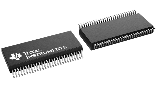
SN74LVCH16543A Series
16-Bit Registered Transceiver With 3-State Outputs
Manufacturer: Texas Instruments
Catalog
16-Bit Registered Transceiver With 3-State Outputs
Key Features
• Member of the Texas Instruments Widebus™ FamilyOperates From 1.65 V to 3.6 VInputs Accept Voltages to 5.5 VMax tpdof 5.4 ns at 3.3 VTypical VOLP(Output Ground Bounce)<0.8 V at VCC= 3.3 V, TA= 25°CTypical VOHV(Output VOHUndershoot)>2 V at VCC= 3.3 V, TA= 25°CIoffSupports Partial-Power-Down Mode OperationSupports Mixed-Mode Signal Operation on All Ports (5-V Input/Output Voltage With 3.3-V VCC)Bus Hold on Data Inputs Eliminates the Need for External Pullup/Pulldown ResistorsLatch-Up Performance Exceeds 250 mA Per JESD 17ESD Protection Exceeds JESD 222000-V Human-Body Model (A114-A)200-V Machine Model (A115-A)1000-V Charged-Device Model (C101)Widebus is a trademark of Texas Instruments.Member of the Texas Instruments Widebus™ FamilyOperates From 1.65 V to 3.6 VInputs Accept Voltages to 5.5 VMax tpdof 5.4 ns at 3.3 VTypical VOLP(Output Ground Bounce)<0.8 V at VCC= 3.3 V, TA= 25°CTypical VOHV(Output VOHUndershoot)>2 V at VCC= 3.3 V, TA= 25°CIoffSupports Partial-Power-Down Mode OperationSupports Mixed-Mode Signal Operation on All Ports (5-V Input/Output Voltage With 3.3-V VCC)Bus Hold on Data Inputs Eliminates the Need for External Pullup/Pulldown ResistorsLatch-Up Performance Exceeds 250 mA Per JESD 17ESD Protection Exceeds JESD 222000-V Human-Body Model (A114-A)200-V Machine Model (A115-A)1000-V Charged-Device Model (C101)Widebus is a trademark of Texas Instruments.
Description
AI
This 16-bit registered transceiver is designed for 1.65-V to 3.6-V VCCoperation.
The SN74LVCH16543A can be used as two 8-bit transceivers or one 16-bit transceiver. Separate latch-enable (LEAB\ or LEBA\) and output-enable (OEAB\ or OEBA\) inputs are provided for each register, to permit independent control in either direction of data flow.
The A-to-B enable (CEAB\) input must be low to enter data from A or to output data from B. If CEAB\ is low and LEAB is low, the A-to-B latches are transparent; a subsequent low-to-high transition of LEAB\ puts the A latches in the storage mode. With CEAB\ and OEAB\ both low, the 3-state B outputs are active and reflect the data present at the output of the A latches. Data flow from B to A is similar, but requires using the CEBA\, LEBA\, and OEBA\ inputs.
To ensure the high-impedance state during power up or power down, OE\ should be tied to VCCthrough a pullup resistor; the minimum value of the resistor is determined by the current-sinking capability of the driver.
Inputs can be driven from either 3.3-V or 5-V devices. This feature allows the use of these devices as translators in a mixed 3.3-V/5-V system environment.
This device is fully specified for partial-power-down applications using Ioff. The Ioffcircuitry disables the outputs, preventing damaging current backflow through the device when it is powered down.
Active bus-hold circuitry is provided to hold unused or floating data inputs at a valid logic level. Use of pullup or pulldown resistors with the bus-hold circuitry is not recommended. The bus-hold circuitry is part of the input circuit and is not disabled by OE\ or DIR.


