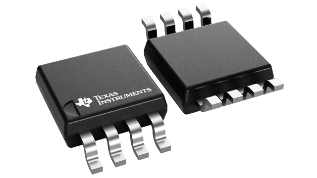
SN65LVDS179-EP Series
Enhanced product high-speed differential line drivers and receivers
Manufacturer: Texas Instruments
Catalog
Enhanced product high-speed differential line drivers and receivers
Key Features
• Controlled BaselineOne Assembly/Test Site, One Fabrication SiteEnhanced Diminishing Manufacturing Sources (DMS) SupportEnhanced Product-Change NotificationQualification Pedigree(1)Meet or Exceed the Requirements of ANSI TIA/EIA-644-1995 StandardSignaling Rates up to 400 MbpsBus-Terminal ESD Exceeds 12 kVOperates From a Single 3.3-V SupplyLow-Voltage Differential Signaling With Typical Output Voltages of 350 mV and a 100-LoadPropagation Delay TimesDriver: 1.7 ns TypReceiver: 3.7 ns TypPower Dissipation at 200 MHzDriver: 25 mW TypicalReceiver: 60 mW TypicalLVTTL Input Levels Are 5-V TolerantReceiver Maintains High Input Impedance With VCC< 1.5 VReceiver Has Open-Circuit Fail Safe(1)Component qualification in accordance with JEDEC and industry standards to ensure reliable operation over an extended temperature range. This includes, but is not limited to, Highly Accelerated Stress Test (HAST) or biased 85/85, temperature cycle, autoclave or unbiased HAST, electromigration, bond intermetallic life, and mold compound life. Such qualification testing should not be viewed as justifying use of this component beyond specified performance and environmental limits.Controlled BaselineOne Assembly/Test Site, One Fabrication SiteEnhanced Diminishing Manufacturing Sources (DMS) SupportEnhanced Product-Change NotificationQualification Pedigree(1)Meet or Exceed the Requirements of ANSI TIA/EIA-644-1995 StandardSignaling Rates up to 400 MbpsBus-Terminal ESD Exceeds 12 kVOperates From a Single 3.3-V SupplyLow-Voltage Differential Signaling With Typical Output Voltages of 350 mV and a 100-LoadPropagation Delay TimesDriver: 1.7 ns TypReceiver: 3.7 ns TypPower Dissipation at 200 MHzDriver: 25 mW TypicalReceiver: 60 mW TypicalLVTTL Input Levels Are 5-V TolerantReceiver Maintains High Input Impedance With VCC< 1.5 VReceiver Has Open-Circuit Fail Safe(1)Component qualification in accordance with JEDEC and industry standards to ensure reliable operation over an extended temperature range. This includes, but is not limited to, Highly Accelerated Stress Test (HAST) or biased 85/85, temperature cycle, autoclave or unbiased HAST, electromigration, bond intermetallic life, and mold compound life. Such qualification testing should not be viewed as justifying use of this component beyond specified performance and environmental limits.
Description
AI
The SN65LVDS179, SN65LVDS180, SN65LVDS050, and SN65LVDS051 are differential line drivers and receivers that use low-voltage differential signaling (LVDS) to achieve signaling rates as high as 400 Mbps. The TIA/EIA-644 standard compliant electrical interface provides a minimum differential output voltage magnitude of 247 mV into a 100-load, and receipt of 100-mV signals with up to 1 V of ground potential difference between a transmitter and receiver.
The intended application of this device and signaling technique is for point-to-point baseband data transmission over controlled impedance media of approximately 100-characteristic impedance. The transmission media may be printed circuit board traces, backplanes, or cables. (Note: The ultimate rate and distance of data transfer is dependent upon the attenuation characteristics of the media, the noise coupling to the environment, and other application specific characteristics.)
The devices offer various driver, receiver, and enabling combinations in industry standard footprints. Since these devices are intended for use in simplex or distributed simplex bus structures, the driver enable function does not put the differential outputs into a high-impedance state, but rather disconnects the input and reduces the quiescent power used by the device. (For these functions with a high-impedance driver output, see the SN65LVDM series of devices.) All devices are characterized for operation from -55°C to 125°C.


