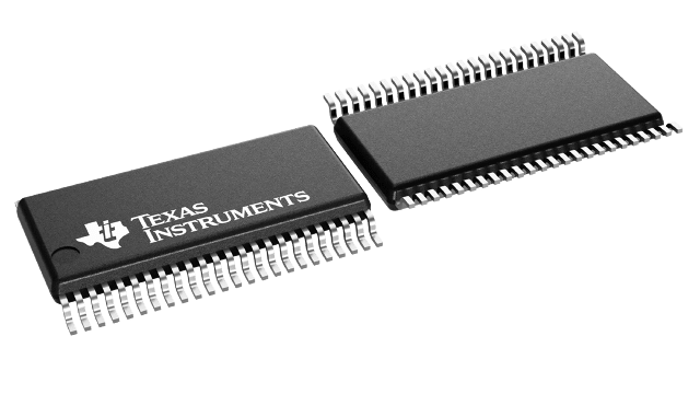
SN74ALVTH16244 Series
16-ch, 2.3-V to 3.6-V buffers with bus-hold, TTL-compatible CMOS inputs and 3-state outputs
Manufacturer: Texas Instruments
Catalog
16-ch, 2.3-V to 3.6-V buffers with bus-hold, TTL-compatible CMOS inputs and 3-state outputs
Key Features
• Members of the Texas InstrumentsWidebusTMFamilyState-of-the-Art Advanced BiCMOS Technology (ABT) Design for 3.3-V Operation and Low Static-Power Dissipation5-V I/O CompatibleHigh Drive Capability (-32 mA/64 mA)Support Mixed-Mode Signal Operation (5-V Input and Output Voltages With 3.3-V VCC)Support Unregulated Battery Operation Down to 2.3 VTypical VOLP(Output Ground Bounce) < 0.8 V at VCC= 3.3 V, TA= 25°CAuto3-State Eliminates Bus Current Loading When Voltage at the Output Exceeds VCCIoffand Power-Up 3-State Support Hot InsertionBus Hold on Data Inputs Eliminates the Need for External Pullup/Pulldown ResistorsLatch-Up Performance Exceeds 250 mA Per JESD 17ESD Protection Exceeds 2000 V Per MIL-STD-883, Method 3015; Exceeds 200 V Using Machine Model (C = 200 pF, R = 0)Package Options Include Plastic 300-mil Shrink Small-Outline (DL), Thin Shrink Small-Outline (DGG), Thin Very Small-Outline (DGV) Packages, and 380-mil Fine-Pitch Ceramic Flat (WD) PackageNOTE: For tape and reel order entry:The DGGR package is abbreviated to GR, andthe DGVR package is abbreviated to VR.Widebus is a trademark of Texas Instruments Incorporated.Members of the Texas InstrumentsWidebusTMFamilyState-of-the-Art Advanced BiCMOS Technology (ABT) Design for 3.3-V Operation and Low Static-Power Dissipation5-V I/O CompatibleHigh Drive Capability (-32 mA/64 mA)Support Mixed-Mode Signal Operation (5-V Input and Output Voltages With 3.3-V VCC)Support Unregulated Battery Operation Down to 2.3 VTypical VOLP(Output Ground Bounce) < 0.8 V at VCC= 3.3 V, TA= 25°CAuto3-State Eliminates Bus Current Loading When Voltage at the Output Exceeds VCCIoffand Power-Up 3-State Support Hot InsertionBus Hold on Data Inputs Eliminates the Need for External Pullup/Pulldown ResistorsLatch-Up Performance Exceeds 250 mA Per JESD 17ESD Protection Exceeds 2000 V Per MIL-STD-883, Method 3015; Exceeds 200 V Using Machine Model (C = 200 pF, R = 0)Package Options Include Plastic 300-mil Shrink Small-Outline (DL), Thin Shrink Small-Outline (DGG), Thin Very Small-Outline (DGV) Packages, and 380-mil Fine-Pitch Ceramic Flat (WD) PackageNOTE: For tape and reel order entry:The DGGR package is abbreviated to GR, andthe DGVR package is abbreviated to VR.Widebus is a trademark of Texas Instruments Incorporated.
Description
AI
The 'ALVTH16244 devices are 16-bit buffers/line drivers designed for 2.5-V or 3.3-V VCCoperation, but with the capability to provide a TTL interface to a 5-V system environment. These devices can be used as four 4-bit buffers, two 8-bit buffers, or one 16-bit buffer.
Active bus-hold circuitry is provided to hold unused or floating data inputs at a valid logic level.
When VCCis between 0 and 1.2 V, the device is in the high-impedance state during power up or power down. However, to ensure the high-impedance state above 1.2 V, the output-enable (OE\) input should be tied to VCCthrough a pullup resistor; the minimum value of the resistor is determined by the current-sinking capability of the driver.
These devices are fully specified for hot-insertion applications using Ioffand power-up 3-state. The Ioffcircuitry disables the outputs, preventing damaging current backflow through the devices when they are powered down. The power-up 3-state circuitry places the outputs in the high-impedance state during power up and power down, which prevents driver conflict.
The SN54ALVTH16244 is characterized for operation over the full military temperature range of -55°C to 125°C. The SN74ALVTH16244 is characterized for operation from -40°C to 85°C.


