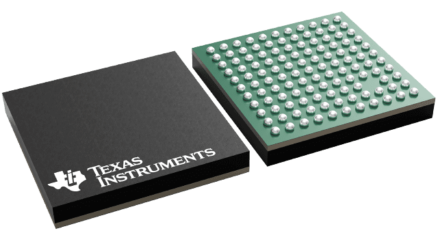
TPS65921 Series
Integrated Power Management IC (PMIC) with 3 DC/DC's, 4 LDOs, USB HS Transceiver
Manufacturer: Texas Instruments
Catalog
Integrated Power Management IC (PMIC) with 3 DC/DC's, 4 LDOs, USB HS Transceiver
Description
AI
The TPS65921 device is a highly integrated power-management circuit (IC) that supports the power and peripheral requirements of the OMAP application processors. The device contains power management, a universal serial bus (USB) high-speed (HS) transceiver, an analog-to-digital converter (ADC), a real-time clock (RTC), a keypad interface, and an embedded power control (EPC). The power portion of the device contains three buck converters, two controllable by a dedicated SmartReflex class-3 interface, multiple low-dropout (LDO) regulators, an EPC to manage the power-sequencing requirements of OMAP, and an RTC module. The USB module provides an HS 2.0 transceiver suitable for direct connection to the OMAP universal transceiver macrocell interface (UTMI) + low pin interface (ULPI) with an integrated charge pump (CP).
The device also provides auxiliary modules: ADC, keypad interface, and general-purpose inputs/outputs (GPIOs) muxed with the JTAG functions. The keypad interface implements a built-in scanning algorithm to decode hardware-based key presses and to reduce software use, with multiple additional GPIOs that can be used as interrupts when they are configured as inputs.


