ADS52J65 Series
8-channel 16-bit 125-MSPS analog-to-digital converter (ADC) with JESD204B interface
Manufacturer: Texas Instruments
Catalog
8-channel 16-bit 125-MSPS analog-to-digital converter (ADC) with JESD204B interface
Key Features
• 16-Bit Resolution, Idle SNR: 80 dBFS70 mW/Ch at 125 MSPS, 4-CH per Lane45 mW/Ch at 62.5 MSPS, 8-CH per LaneFull-Scale Input: 2 VPPFull-Scale SNR: 78 dBFS at fin= 10 MHzFull-Scale SFDR: –85 dBc at fin= 10 MHzAnalog Input –3 dB Bandwidth = 250 MHzMaximum Input Signal Frequency for 2 VPPInput = 130 MHzFast and Consistent Overload RecoveryAdvanced Digital FeaturesAutomatic DC Offset CorrectionDigital AverageDigital I/Q DemodulatorFractional Decimation Filter M = 1 to 63 With Increments of 0.25Data Output Rate Reduction After Decimation64 mW/Ch at 80 MSPS and Decimation = 2On-Chip RAM With 32 Preset ProfilesJESD204B Subclass 0, 1, and 22, 4, or 8 Channels per JESD Lane10-Gbps JESD InterfaceSupports lane rate up to 12.8 Gbps for short trace length (< 5 Inch)64-Pin Non-Magnetic 9 × 9-mm Package16-Bit Resolution, Idle SNR: 80 dBFS70 mW/Ch at 125 MSPS, 4-CH per Lane45 mW/Ch at 62.5 MSPS, 8-CH per LaneFull-Scale Input: 2 VPPFull-Scale SNR: 78 dBFS at fin= 10 MHzFull-Scale SFDR: –85 dBc at fin= 10 MHzAnalog Input –3 dB Bandwidth = 250 MHzMaximum Input Signal Frequency for 2 VPPInput = 130 MHzFast and Consistent Overload RecoveryAdvanced Digital FeaturesAutomatic DC Offset CorrectionDigital AverageDigital I/Q DemodulatorFractional Decimation Filter M = 1 to 63 With Increments of 0.25Data Output Rate Reduction After Decimation64 mW/Ch at 80 MSPS and Decimation = 2On-Chip RAM With 32 Preset ProfilesJESD204B Subclass 0, 1, and 22, 4, or 8 Channels per JESD Lane10-Gbps JESD InterfaceSupports lane rate up to 12.8 Gbps for short trace length (< 5 Inch)64-Pin Non-Magnetic 9 × 9-mm Package
Description
AI
The 8-channel, 16-bit ADS52J65 analog-to-digital converter (ADC) uses CMOS process and innovative circuit techniques. It is designed to operate at low power and give very high signal-to-noise ratio (SNR) performance with a 2-Vpp full-scale input. The device gives 80-dBFS idle SNR and 78-dBFS full-scale SNR at 5 MHz. The large input bandwidth of 250 MHz makes the device suitable for a wide range of applications, such as high frequency medical ultrasound, magnetic resonance imaging, multi-channel data acquisition, flow cytometry, flow cytometer, and hematology analyzer. The ADC integrates an internal reference trimmed to match across devices.
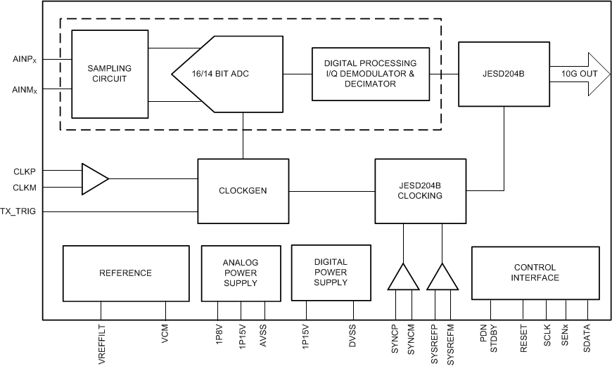
ADS52J65 has advanced digital features, including a digital I/Q demodulator with fractional decimation filter. The ADC data from each channel is encoded using an 8B to 10B format and is sent as a SerDes data stream using current-mode logic (CML) output buffers, as per the JESD204B standard. The ADC data from all eight channels can be output over a single CML buffer (1-lane SerDes) with the data rate limited to a maximum of 12.8 Gbps. Using SerDes outputs reduces the number of interface lines. This, together with the low-power design, enables eight channels to be packaged in a 9-mm × 9-mm VQFN allowing high system integration densities. ADS52J65 also supports modes where all ADC data is sent over four CML buffers (4-Lane SerDes), reducing the SerDes data rate per lane for low-cost FPGAs.
The ADS52J65 is available in a non-magnetic VQFN package that does not create any magnetic artifact. The device is specified over –40°C to +85°C.


