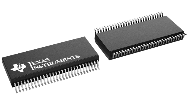
SN74ALVCH16501 Series
18-bit universal bus transceiver with 3-state outputs
Manufacturer: Texas Instruments
Catalog
18-bit universal bus transceiver with 3-state outputs
Key Features
• Member of the Texas Instruments Widebus™ FamilyUBT™ Transceiver Combines D-Type Latches and D-Type Flip-Flops for Operation in Transparent, Latched, or Clocked ModesOperates From 1.65 V to 3.6 VMax tpdof 3.9 ns at 3.3 V±24-mA Output Drive at 3.3 VBus Hold on Data Inputs Eliminates the Need for External Pullup/Pulldown ResistorsLatch-Up Performance Exceeds 250 mA Per JESD 17ESD Protection Exceeds JESD 222000-V Human-Body Model (A114-A)200-V Machine Model (A115-A)Widebus, UBT are trademarks of Texas Instruments.Member of the Texas Instruments Widebus™ FamilyUBT™ Transceiver Combines D-Type Latches and D-Type Flip-Flops for Operation in Transparent, Latched, or Clocked ModesOperates From 1.65 V to 3.6 VMax tpdof 3.9 ns at 3.3 V±24-mA Output Drive at 3.3 VBus Hold on Data Inputs Eliminates the Need for External Pullup/Pulldown ResistorsLatch-Up Performance Exceeds 250 mA Per JESD 17ESD Protection Exceeds JESD 222000-V Human-Body Model (A114-A)200-V Machine Model (A115-A)Widebus, UBT are trademarks of Texas Instruments.
Description
AI
This 18-bit universal bus transceiver is designed for 1.65-V to 3.6-V VCCoperation.
Data flow in each direction is controlled by output-enable (OEAB and OEBA)\, latch-enable (LEAB and LEBA), and clock (CLKAB and CLKBA) inputs. For A-to-B data flow, the device operates in the transparent mode when LEAB is high. When LEAB is low, the A data is latched if CLKAB is held at a high or low logic level. If LEAB is low, the A data is stored in the latch/flip-flop on the low-to-high transition of CLKAB. When OEAB is high, the outputs are active. When OEAB is low, the outputs are in the high-impedance state.
Data flow for B to A is similar to that of A to B, but uses OEBA\, LEBA, and CLKBA. The output enables are complementary (OEAB is active high and OEBA\ is active low).
To ensure the high-impedance state during power up or power down, OEBA\ should be tied to VCCthrough a pullup resistor and OEAB should be tied to GND through a pulldown resistor; the minimum value of the resistor is determined by the current-sinking capability of the driver.
Active bus-hold circuitry holds unused or undriven inputs at a valid logic state. Use of pullup or pulldown resistors with the bus-hold circuitry is not recommended.


