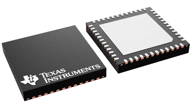
LMK5B12204 Series
Ultra-low jitter clock generator with network synchronization and BAW technology
Manufacturer: Texas Instruments
Catalog
Ultra-low jitter clock generator with network synchronization and BAW technology
Key Features
• One Digital Phase-Locked Loop (DPLL) With:Hitless Switching: ±50-ps Phase TransientProgrammable Loop Bandwidth With FastlockStandards-Compliant Synchronization and Holdover Using a Low-Cost TCXO/OCXOTwo Analog Phase-Locked Loops (APLLs) With Industry-Leading Jitter Performance:50-fs RMS Jitter at 312.5 MHz (APLL1)125-fs RMS Jitter at 155.52 MHz (APLL2)Two Reference Clock InputsPriority-Based Input SelectionDigital Holdover on Loss of ReferenceFour Clock Outputs with Programmable DriversUp to Four Different Output FrequenciesAC-LVDS, AC-CML, AC-LVPECL, HCSL, and 1.8-V LVCMOS Output FormatsEEPROM / ROM for Custom Clocks on Power-UpFlexible Configuration Options1 Hz (1 PPS) to 800 MHz on InputXO/TCXO/OCXO Input: 10 to 100 MHzDCO Mode: < 0.001 ppb/Step for Precise Clock Steering (IEEE 1588 PTP Slave)Advanced Clock Monitoring and StatusI2C or SPI InterfacePSNR: –83 dBc (50-mVpp Noise on 3.3-V Supply)3.3-V Supply With 1.8-V, 2.5-V, or 3.3-V OutputsIndustrial Temperature Range: –40 °C to +85 °COne Digital Phase-Locked Loop (DPLL) With:Hitless Switching: ±50-ps Phase TransientProgrammable Loop Bandwidth With FastlockStandards-Compliant Synchronization and Holdover Using a Low-Cost TCXO/OCXOTwo Analog Phase-Locked Loops (APLLs) With Industry-Leading Jitter Performance:50-fs RMS Jitter at 312.5 MHz (APLL1)125-fs RMS Jitter at 155.52 MHz (APLL2)Two Reference Clock InputsPriority-Based Input SelectionDigital Holdover on Loss of ReferenceFour Clock Outputs with Programmable DriversUp to Four Different Output FrequenciesAC-LVDS, AC-CML, AC-LVPECL, HCSL, and 1.8-V LVCMOS Output FormatsEEPROM / ROM for Custom Clocks on Power-UpFlexible Configuration Options1 Hz (1 PPS) to 800 MHz on InputXO/TCXO/OCXO Input: 10 to 100 MHzDCO Mode: < 0.001 ppb/Step for Precise Clock Steering (IEEE 1588 PTP Slave)Advanced Clock Monitoring and StatusI2C or SPI InterfacePSNR: –83 dBc (50-mVpp Noise on 3.3-V Supply)3.3-V Supply With 1.8-V, 2.5-V, or 3.3-V OutputsIndustrial Temperature Range: –40 °C to +85 °C
Description
AI
The LMK5B12204 is high-performance network synchronizer clock device that provides jitter cleaning, clock generation, advanced clock monitoring, and superior hitless switching performance to meet the stringent timing requirements of communications infrastructure and industrial applications. The ultra-low jitter and high power supply noise rejection (PSNR) of the device can reduce bit error rates (BER) in high-speed serial links.
The device can generate output clocks with 50-fs RMS jitter using TI’s proprietary Bulk Acoustic Wave (BAW) VCO technology, independent of the jitter and frequency of the XO and reference inputs.


