Catalog
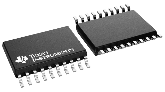
SN74AHC8541
Key Features
• Operating Range of 2 V to 5.5 V VCC8-Bit Inverting/Non-Inverting Outputs20-Pin Thin Shrink Small-Outline Package[TSSOP (PW)] and 20-Pin Plastic Dual-In-LinePackage [PDIP (N)]Operating Range of 2 V to 5.5 V VCC8-Bit Inverting/Non-Inverting Outputs20-Pin Thin Shrink Small-Outline Package[TSSOP (PW)] and 20-Pin Plastic Dual-In-LinePackage [PDIP (N)]
Description
AI
The SN74AHC8541 8-bit inverting/non-inverting buffers are ideal for driving bus lines or buffer memory address registers. These devices feature inputs and outputs on opposite sides of the package to facilitate printed circuit board layout.
All outputs are in the high-impedance state (disabled) when the output-enable (OE) input is high. WhenOEis low, the respective gate passes the data from the D input to its Y output.
The T/Cinput selects inverting or non-inverting data transfer. When the T/Cinput is high, it provides non-inverting buffers. When the T/Cinput is low, it provides inverting buffers when they are not in the high-impedance state.
To ensure the high-impedance state during power up or power down,OEshould be tied to VCCthrough a pullup resistor; the minimum value of the resistor is determined by the current-sinking capability of the driver.


