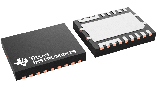
CSD95492QVM Series
20A Synchronous Buck NexFET Smart Power Stage in small 4x5 SON Package
Manufacturer: Texas Instruments
Catalog
20A Synchronous Buck NexFET Smart Power Stage in small 4x5 SON Package
Key Features
• 20-A Continuous Operating Current CapabilityOver 94% System Efficiency at 12 AHigh-Frequency Operation (up to 1.25 MHz)Diode Emulation FunctionTemperature Compensated Bi-Directional Current SenseAnalog Temperature OutputFault Monitoring3.3-V and 5-V PWM Signal CompatibleTri-State PWM InputIntegrated Bootstrap SwitchOptimized Dead Time for Shoot-Through ProtectionHigh-Density VSON 4-mm × 5-mm FootprintUltra-Low-Inductance PackageSystem Optimized PCB FootprintRoHS Compliant – Lead-Free Terminal PlatingHalogen Free20-A Continuous Operating Current CapabilityOver 94% System Efficiency at 12 AHigh-Frequency Operation (up to 1.25 MHz)Diode Emulation FunctionTemperature Compensated Bi-Directional Current SenseAnalog Temperature OutputFault Monitoring3.3-V and 5-V PWM Signal CompatibleTri-State PWM InputIntegrated Bootstrap SwitchOptimized Dead Time for Shoot-Through ProtectionHigh-Density VSON 4-mm × 5-mm FootprintUltra-Low-Inductance PackageSystem Optimized PCB FootprintRoHS Compliant – Lead-Free Terminal PlatingHalogen Free
Description
AI
The CSD95492QVM NexFET™ power stage is a highly optimized design for use in a high-power, high-density synchronous buck converter. This product integrates the driver IC and power MOSFETs to complete the power stage switching function. This combination produces high-current, high-efficiency, and high-speed switching capability in a small 4-mm × 5-mm outline package. It also integrates the accurate current sensing and temperature sensing functionality to simplify system design and improve accuracy. In addition, the PCB footprint has been optimized to help reduce design time and simplify the completion of the overall system design.
The CSD95492QVM NexFET™ power stage is a highly optimized design for use in a high-power, high-density synchronous buck converter. This product integrates the driver IC and power MOSFETs to complete the power stage switching function. This combination produces high-current, high-efficiency, and high-speed switching capability in a small 4-mm × 5-mm outline package. It also integrates the accurate current sensing and temperature sensing functionality to simplify system design and improve accuracy. In addition, the PCB footprint has been optimized to help reduce design time and simplify the completion of the overall system design.


