Catalog
Monolithic Sample and Hold Circuit
Key Features
• Operates from ±5V to ±18V suppliesLess than 10 μs acquisition timeTTL, PMOS, CMOS compatible logic input0.5 mV typical hold step at Ch= 0.01 μFLow input offset0.002% gain accuracyLow output noise in hold modeInput characteristics do not change during hold modeHigh supply rejection ratio in sample or holdWide bandwidthAll trademarks are the property of their respective owners.Operates from ±5V to ±18V suppliesLess than 10 μs acquisition timeTTL, PMOS, CMOS compatible logic input0.5 mV typical hold step at Ch= 0.01 μFLow input offset0.002% gain accuracyLow output noise in hold modeInput characteristics do not change during hold modeHigh supply rejection ratio in sample or holdWide bandwidthAll trademarks are the property of their respective owners.
Description
AI
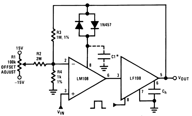
The LF198 is a monolithic sample-and-hold circuit which utilizes BI-FET technology to obtain ultra-high dc accuracy with fast acquisition of signal and low droop rate. Operating as a unity gain follower, dc gain accuracy is 0.002% typical and acquisition time is as low as 6 μs to 0.01%. A bipolar input stage is used to achieve low offset voltage and wide bandwidth. Input offset adjust is accomplished with a single pin, and does not degrade input offset drift. The wide bandwidth allows the LF198 to be included inside the feedback loop of 1 MHz op amps without having stability problems. Input impedance of 1010Ω allows high source impedances to be used without degrading accuracy.
P-channel junction FET's are combined with bipolar devices in the output amplifier to give droop rates as low as 5 mV/min with a 1 μF hold capacitor. The JFET's have much lower noise than MOS devices used in previous designs and do not exhibit high temperature instabilities. The overall design specifies no feed-through from input to output in the hold mode, even for input signals equal to the supply voltages.
Logic inputs on the LF198 are fully differential with low input current, allowing direct connection to TTL, PMOS, and CMOS. Differential threshold is 1.4V. The LF198 will operate from ±5V to ±18V supplies.


