LMK1D1208P Series
8-channel output 1.8-V, 2.5-V, and 3.3-V LVDS buffer with pin control
Manufacturer: Texas Instruments
Catalog
8-channel output 1.8-V, 2.5-V, and 3.3-V LVDS buffer with pin control
Key Features
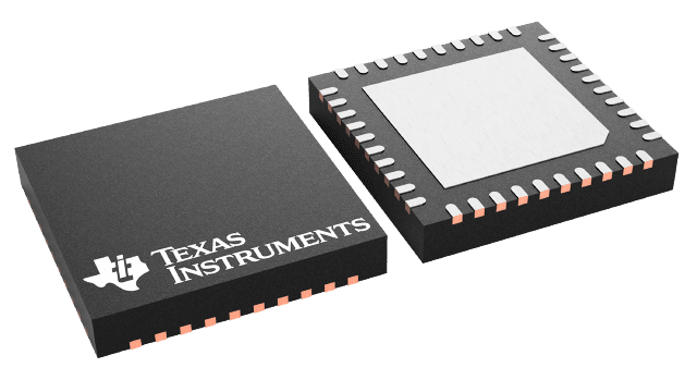
• High-performance LVDS clock buffer family with 2 inputs and 8 outputs (2:8)Output frequency up to 2 GHzHardware pins for individual output enable/disableSupply voltage: 1.8 V / 2.5 V / 3.3 V ± 5%Low additive jitter: < 60 fs rms maximum in 12 kHz to 20 MHz at 156.25 MHzVery low phase noise floor: -164 dBc/Hz (typical)Very low propagation delay: < 575 ps maximumOutput skew: 20 ps maximumFail-safe inputsUniversal inputs accept LVDS, LVPECL, LVCMOS, HCSL and CMLLVDS reference voltage, V AC_REF, available for capacitive-coupled inputsIndustrial temperature range: –40°C to 105°CPackages available:6-mm × 6-mm, 40-pin VQFN (RHA)High-performance LVDS clock buffer family with 2 inputs and 8 outputs (2:8)Output frequency up to 2 GHzHardware pins for individual output enable/disableSupply voltage: 1.8 V / 2.5 V / 3.3 V ± 5%Low additive jitter: < 60 fs rms maximum in 12 kHz to 20 MHz at 156.25 MHzVery low phase noise floor: -164 dBc/Hz (typical)Very low propagation delay: < 575 ps maximumOutput skew: 20 ps maximumFail-safe inputsUniversal inputs accept LVDS, LVPECL, LVCMOS, HCSL and CMLLVDS reference voltage, V AC_REF, available for capacitive-coupled inputsIndustrial temperature range: –40°C to 105°CPackages available:6-mm × 6-mm, 40-pin VQFN (RHA)
Description
AI
The LMK1D1208P clock buffer distributes one of two selectable clock inputs (IN0 and IN1) to 8 pairs of differential LVDS clock outputs (OUT0 through OUT7) with minimum skew for clock distribution. The inputs can be either LVDS, LVPECL, LVCMOS, HCSL, or CML.
The LMK1D1208P is specifically designed for driving 50-Ω transmission lines. When driving inputs in single-ended mode, apply the appropriate bias voltage to the unused negative input pin. The IN_SEL pin selects the input which is routed to the outputs. The part supports a fail-safe input function. The device further incorporates an input hysteresis which prevents random oscillation of the outputs in the absence of an input signal.
Each LVDS differential output is enabled by setting the corresponding OEx pin to a logic high 1. If this pin is set to a logic low 0, the output is disabled in a Hi-Z state resulting in reduced power consumption.
The device operates in a 1.8-V, 2.5-V, or 3.3-V supply environment and is characterized from –40°C to 105°C (ambient temperature).


