SN65LVDS315 Series
8-bit parallel RGB to MIPI® CSI-1 or SMIA CCP transmitter & serializer
Manufacturer: Texas Instruments
Catalog
8-bit parallel RGB to MIPI® CSI-1 or SMIA CCP transmitter & serializer
Key Features
• MIPI CSI-1 and SMIA CCP SupportConnects Directly to OMAP CSI Interface4×4 mm QFN PackageESD Rating >3 kV (HBM) Camera Input Portsand >2 kV (HBM) All Other PortsPixel Clock Range 3.5–27 MHzThree Operating Modes to Conserve PowerActive Mode VGA Camera 30 fps: 7 mATypical Shutdown and Standby: 0.5 µAOperating Temperature Range –40°Cto 85°CInput Data Voltage Range From 1.8 V to 3.3 VEMIMIPI CSI-1 and SMIA CCP SupportConnects Directly to OMAP CSI Interface4×4 mm QFN PackageESD Rating >3 kV (HBM) Camera Input Portsand >2 kV (HBM) All Other PortsPixel Clock Range 3.5–27 MHzThree Operating Modes to Conserve PowerActive Mode VGA Camera 30 fps: 7 mATypical Shutdown and Standby: 0.5 µAOperating Temperature Range –40°Cto 85°CInput Data Voltage Range From 1.8 V to 3.3 VEMI
Description
AI
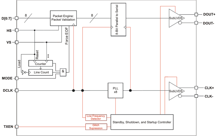
The SN65LVDS315 is a camera serializer that converts 8-bit parallel camera data into MIPI-CSI1 or SMIA CCP compliant serial signals.
The device converts the parallel 8-bit data to two sub-low-voltage differential signaling (SubLVDS) serial data and clock output. Meanwhile the serialized data is presented on the differential serial data output DOUT with a differential clock signal on output CLK. Where The frequency of CLK is 8x DCLK input pixel clock rate.
The SN65LVDS315 supports three power modes (Shutdown, standby and active) to conserve power.
All CMOS inputs offer failsafe operation to protect the input from damage during power up and to avoid current flow into the device inputs during power up. The core supply of the SN65LVDS315 is 1.8 V. To provide greater flexibility, the camera data inputs support a supply range from 1.8 V to 3.3 V and the device is characterized for operation over ambient air temperatures of –40°C to 85°C.


