SN74AUC2G240 Series
2-ch, 0.8-V to 2.7-V high speed inverters with 3-state outputs
Manufacturer: Texas Instruments
Catalog
2-ch, 0.8-V to 2.7-V high speed inverters with 3-state outputs
Key Features
• Available in the Texas Instruments NanoFree™ PackageOptimized for 1.8-V Operation and Is 3.6-V I/O Tolerant to Support Mixed-Mode Signal OperationIoffSupports Partial-Power-Down Mode OperationSub-1-V OperableMax tpdof 1.8 ns at 1.8 VLow Power Consumption, 10 µA at 1.8 V±8-mA Output Drive at 1.8 VLatch-Up Performance Exceeds 100 mA Per JESD 78, Class IIESD Protection Exceeds JESD 222000-V Human-Body Model (A114-A)200-V Machine Model (A115-A)1000-V Charged-Device Model (C101)NanoFree is a trademark of Texas Instruments.Available in the Texas Instruments NanoFree™ PackageOptimized for 1.8-V Operation and Is 3.6-V I/O Tolerant to Support Mixed-Mode Signal OperationIoffSupports Partial-Power-Down Mode OperationSub-1-V OperableMax tpdof 1.8 ns at 1.8 VLow Power Consumption, 10 µA at 1.8 V±8-mA Output Drive at 1.8 VLatch-Up Performance Exceeds 100 mA Per JESD 78, Class IIESD Protection Exceeds JESD 222000-V Human-Body Model (A114-A)200-V Machine Model (A115-A)1000-V Charged-Device Model (C101)NanoFree is a trademark of Texas Instruments.
Description
AI
This dual buffer/driver is operational at 0.8-V to 2.7-V VCC, but is designed specifically for 1.65-V to 1.95-V VCCoperation.
The SN74AUC2G240 is designed specifically to improve the performance and density of 3-state memory address drivers, clock drivers, and bus-oriented receivers and transmitters.
This device is organized as two 1-bit buffers/drivers with separate output-enable (OE) inputs. WhenOEis low, the device passes data from the A input to the Y output. WhenOEis high, the outputs are in the high-impedance state.
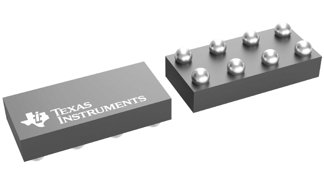
NanoFree™ package technology is a major breakthrough in IC packaging concepts, using the die as the package.
To ensure the high-impedance state during power up or power down,OEshould be tied to VCCthrough a pullup resistor; the minimum value of the resistor is determined by the current-sinking capability of the driver.
This device is fully specified for partial-power-down applications using Ioff. The Ioffcircuitry disables the outputs, preventing damaging current backflow through the device when it is powered down.
For more information about AUC Little Logic devices, please refer to the TI application report,Applications of Texas Instruments AUC Sub-1-V Little Logic Devices,literature number SCEA027.


