TPD5S115 Series
HDMI companion chip with step-Up DC-DC Con-Verter, level shifter, and ESD clamp
Manufacturer: Texas Instruments
Catalog
HDMI companion chip with step-Up DC-DC Con-Verter, level shifter, and ESD clamp
Key Features
• Conforms to HDMI Compliance Tests Without Any External ComponentsSupports HDMI 2.0, HDMI 1.4, and HDMI 1.3 StandardsMatches HDMI Connector Pin MappingInternal DC-DC Converter to Generate 5 V From a Battery Voltage as Low as 2.3 VAuto-Direction Sensing, Level Shifting, and Buffering in the CEC, SDA, and SCL PathsIEC 61000-4-2 (Level 4) System Level ESD ComplianceReverse Current Blocking and Short-Circuit Protection to Protect Against Fault ConditionsIndustrial Temperature Range: –40°C to 85°CConforms to HDMI Compliance Tests Without Any External ComponentsSupports HDMI 2.0, HDMI 1.4, and HDMI 1.3 StandardsMatches HDMI Connector Pin MappingInternal DC-DC Converter to Generate 5 V From a Battery Voltage as Low as 2.3 VAuto-Direction Sensing, Level Shifting, and Buffering in the CEC, SDA, and SCL PathsIEC 61000-4-2 (Level 4) System Level ESD ComplianceReverse Current Blocking and Short-Circuit Protection to Protect Against Fault ConditionsIndustrial Temperature Range: –40°C to 85°C
Description
AI
The TPD5S115 device is an integrated HDMI companion chip solution. The device provides a regulated 5-V output (5VOUT) for sourcing the HDMI power line. The regulated 5-V output supplies up to 55 mA to the HDMI receiver with a current limiting function. The TPD5S115 features two control signals: EN and LS_OE. The control of 5VOUT and the hot plug detect (HPD) circuitry is independent of the LS_OE control signal and is controlled by the EN pin. The EN pin allows the detection scheme (5VOUT + HPD) to be active before turning on the whole HDMI link. The LS_OE activates the internal LDO, CEC, SCL, and SDA buffers only when EN is also activated. This dual stage enable scheme ensures optimized power saving for portable applications.
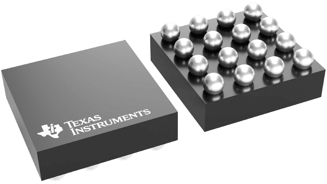
There are three noninverting, bidirectional, voltage level translation circuits for the SDA, SCL, and CEC lines. Each have a common power rail (VCCA) on the A side from 1.1 V to 3.6 V. On the B side, the SCL_B and SDA_B each have an internal 1.75-kΩ pullup connected to the regulated 5-V rail (5VOUT). The DDC (SCL_B and SDA_B) pins meet the I2C specification and drive up to 750-pF loads with the buffers. The CEC_B pin has an internal 27-kΩ pullup to an internal 3.3-V supply. The TPD5S115 exceeds the IEC61000-4-2 (Level 4) ESD protection level. This device features a space saving, 1.72-mm × 1.72-mm, YFF package with 0.4-mm pitch.


