Catalog
SM34020APCM40
Key Features
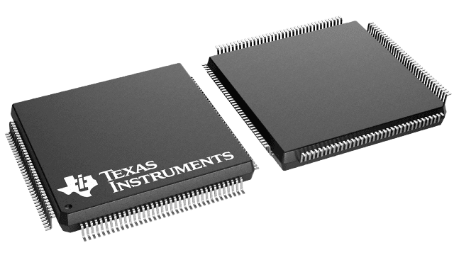
• Class B High-Reliability Processing1-µm CMOS TechnologyCommercial Operating Temperature Range 0°C to 70°CSM34020APCM40 100-ns Instruction Cycle TimeFully Programmable 32-Bit General-Purpose Processor With 512-Megabyte Linear Address Range (Bit Addressable)Second-Generation Graphics System Processor (GSP)Object-Code Compatible With the SM34010Enhanced Instruction SetOptimized Graphics InstructionsCoprocessor InterfacePixel Processing, XY Addressing, and Window Checking Built Into the Instruction SetProgrammable 1-, 2-, 4-, 8-, 16-, or 32-Bit Pixel Size With 16 Boolean and Six Arithmetic Pixel Processing Options (Raster Ops)512-Byte LRU On-Chip Instruction Cache (I-Cache)Optimized DRAM/Video RAM (VRAM) InterfacePage Mode for Burst-Memory OperationsDynamic Bus Sizing (16-Bit and 32-Bit Transfers)Byte-OrientedCASStrobesFlexible Host Processor InterfaceSupports Host TransfersDirect Access to All of the SM34020APCM40 Address SpaceImplicit AddressingPrefetch for Enhanced Read AccessProgrammable CRT ControlComposite Synchronization ModeSeparate Synchronization ModeSynchronization to External SynchronizationDirect Support for Special Features of 1M VRAMsLoad Write MaskLoad Color MaskBlock WriteWrite Using the Write MaskFlexible Multiprocessor Interface144-Pin PCM Quad Flat Package (QFP)Class B High-Reliability Processing1-µm CMOS TechnologyCommercial Operating Temperature Range 0°C to 70°CSM34020APCM40 100-ns Instruction Cycle TimeFully Programmable 32-Bit General-Purpose Processor With 512-Megabyte Linear Address Range (Bit Addressable)Second-Generation Graphics System Processor (GSP)Object-Code Compatible With the SM34010Enhanced Instruction SetOptimized Graphics InstructionsCoprocessor InterfacePixel Processing, XY Addressing, and Window Checking Built Into the Instruction SetProgrammable 1-, 2-, 4-, 8-, 16-, or 32-Bit Pixel Size With 16 Boolean and Six Arithmetic Pixel Processing Options (Raster Ops)512-Byte LRU On-Chip Instruction Cache (I-Cache)Optimized DRAM/Video RAM (VRAM) InterfacePage Mode for Burst-Memory OperationsDynamic Bus Sizing (16-Bit and 32-Bit Transfers)Byte-OrientedCASStrobesFlexible Host Processor InterfaceSupports Host TransfersDirect Access to All of the SM34020APCM40 Address SpaceImplicit AddressingPrefetch for Enhanced Read AccessProgrammable CRT ControlComposite Synchronization ModeSeparate Synchronization ModeSynchronization to External SynchronizationDirect Support for Special Features of 1M VRAMsLoad Write MaskLoad Color MaskBlock WriteWrite Using the Write MaskFlexible Multiprocessor Interface144-Pin PCM Quad Flat Package (QFP)
Description
AI
The SM34020APCM40 graphics system processor (GSP) is the second generation of an advanced high-performance CMOS 32-bit microprocessor optimized for graphics display systems. With a built-in instruction cache (I-cache), the ability to simultaneously access memory and registers, and an instruction set designed to expedite raster graphics operations, the SM34020APCM40 provides user-programmable control of the CRT interface, as well as the memory interface [both standard DRAM and multiport video RAM (VRAM)]. The 4-gigabit (512-megabyte) physical address space is addressable on bit boundaries using variable width data fields (1 to 32 bits). Additional graphics addressing modes support 1-, 2-, 4-, 8-, 16-, and 32-bit-wide pixels.
The SM34020APCM40 graphics system processor (GSP) is the second generation of an advanced high-performance CMOS 32-bit microprocessor optimized for graphics display systems. With a built-in instruction cache (I-cache), the ability to simultaneously access memory and registers, and an instruction set designed to expedite raster graphics operations, the SM34020APCM40 provides user-programmable control of the CRT interface, as well as the memory interface [both standard DRAM and multiport video RAM (VRAM)]. The 4-gigabit (512-megabyte) physical address space is addressable on bit boundaries using variable width data fields (1 to 32 bits). Additional graphics addressing modes support 1-, 2-, 4-, 8-, 16-, and 32-bit-wide pixels.


