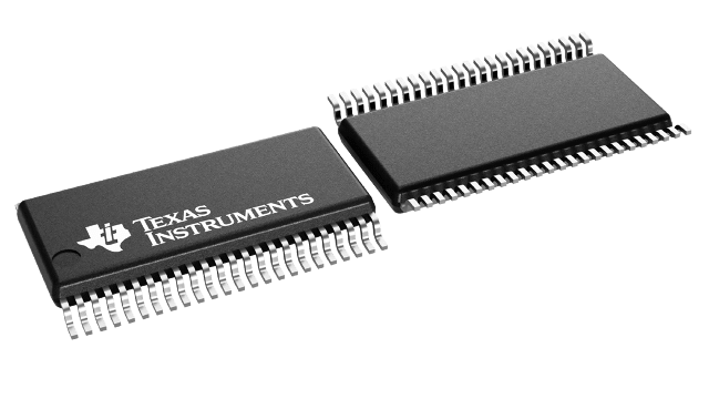
SN74AVC16T245-Q1 Series
16-Bit Dual-Supply Bus Transceiver with Configurable Voltage-Level Shifting and 3-State Outputs
Manufacturer: Texas Instruments
Catalog
16-Bit Dual-Supply Bus Transceiver with Configurable Voltage-Level Shifting and 3-State Outputs
Key Features
• Qualified for Automotive ApplicationsAEC-Q100 Qualified With the Following Results:Device Temperature Grade 1: –40°C to 125°C Ambient Operating Temperature RangeDevice HBM ESD Classification Level H3B (JESD 22 A114-A)Device CDM ESD Classification Level C5 (JESD 22 C101)Control Inputs VIH/VIL Levels Are Referenced to VCCA VoltageVCC Isolation Feature – If Either VCC Input is at GND, Both Ports Are in the High-Impedance StateFully Configurable Dual-Rail Design Allows Each Port to Operate Over the Full 1.2V to 3.6V Power-Supply RangeIoff Supports Partial-Power-Down Mode OperationI/Os Are 4.6V TolerantMaximum Data Rates380Mbps (1.8V to 3.3V Translation)200Mbps (<1.8V to 3.3V Translation)200Mbps (Translate to 2.5V or 1.8V)150Mbps (Translate to 1.5V)100Mbps (Translate to 1.2V)Latch-Up Performance Exceeds 100mA Per JESD 78, Class IIQualified for Automotive ApplicationsAEC-Q100 Qualified With the Following Results:Device Temperature Grade 1: –40°C to 125°C Ambient Operating Temperature RangeDevice HBM ESD Classification Level H3B (JESD 22 A114-A)Device CDM ESD Classification Level C5 (JESD 22 C101)Control Inputs VIH/VIL Levels Are Referenced to VCCA VoltageVCC Isolation Feature – If Either VCC Input is at GND, Both Ports Are in the High-Impedance StateFully Configurable Dual-Rail Design Allows Each Port to Operate Over the Full 1.2V to 3.6V Power-Supply RangeIoff Supports Partial-Power-Down Mode OperationI/Os Are 4.6V TolerantMaximum Data Rates380Mbps (1.8V to 3.3V Translation)200Mbps (<1.8V to 3.3V Translation)200Mbps (Translate to 2.5V or 1.8V)150Mbps (Translate to 1.5V)100Mbps (Translate to 1.2V)Latch-Up Performance Exceeds 100mA Per JESD 78, Class II
Description
AI
This 16-bit noninverting bus transceiver uses two separate configurable power-supply rails. The SN74AVC16T245 device is optimized to operate with VCCA/VCCB set at 1.4V to 3.6V. The device is operational with VCCA/VCCB as low as 1.2V. The A port is designed to track VCCA. VCCA accepts any supply voltage from 1.2V to 3.6V. The B port is designed to track VCCB. VCCB accepts any supply voltage from 1.2V to 3.6V. This allows for universal low-voltage bidirectional translation between any of the 1.2V, 1.5V, 1.8V, 2.5V, and 3.3V voltage nodes.
The SN74AVC16T245 device is designed for asynchronous communication between data buses. The device transmits data from the A bus to the B bus or from the B bus to the A bus, depending on the logic level at the direction-control (DIR) input. The output-enable ( OE) input can be used to disable the outputs so the buses effectively are isolated.
The SN74AVC16T245 control pins (1DIR, 2DIR, 1 OE, and 2 OE) are supplied by VCCA.


