ADS8201 Series
2.2V to 5.5V, Low-Power, 12-Bit, 100kSPS, 8-Channel DAS with PGA and SPI™
Manufacturer: Texas Instruments
Catalog
2.2V to 5.5V, Low-Power, 12-Bit, 100kSPS, 8-Channel DAS with PGA and SPI™
Key Features
• Low-Power, Flexible Supply Range:2.2V to 5.5V Analog Supply1.32mW (100kHz, +VA = 2.2V, +VD = 2.2V)4.5mW (100kHz, +VA = 5V, +VD = 5V)Up to 100kSPS Throughput RateExcellent DC Performance:±0.5 LSB typ, ±1.5 LSB max INL±0.5 LSB typ, ±1.0 LSB max DNL±6 LSB Offset Error at +VA =5V±0.1%FS Gain Error at +VA = 5VFlexible Analog Inputs:True Differential InputDifferential/Unipolar Input Range (0 to VREF)TAG Bit OutputProgrammable Averaging FunctionOnboard, Eight Single-Ended/Four Differential Channel Mux:High Input ImpedanceHigh-Performance PGA (Gain = 1/2/4/8)PGA BreakoutAuto/Manual Channel Select with GainAuto/Manual TriggerMixed Type Partial ScanBuilt-in Hardware Features:On-chip Conversion Clock (CCLK)Hardware/Software ResetProgrammable Status/Polarity for BUSY/INTFlexible I/O:SPI-/DSP™-Compatible Serial InterfaceSeparate I/O Supply (2.2V to 5.5V)Onboard 8×1 FIFO BufferSCLK up to 25MHz (VD = 5V)Multi-Chip Ready and Fully Enabled:GlobalCONVST(Independent ofCS)Power-Down Mode24-Pin 4×4 QFN PackageAPPLICATIONSPortable CommunicationsTransducer InterfacesPortable Medical InstrumentsData Acquisition SystemsGPS ChipsetsDSP is a trademark of Texas Instruments.SPI is a trademark of Motorola Inc.All other trademarks are the property of their respective ownersLow-Power, Flexible Supply Range:2.2V to 5.5V Analog Supply1.32mW (100kHz, +VA = 2.2V, +VD = 2.2V)4.5mW (100kHz, +VA = 5V, +VD = 5V)Up to 100kSPS Throughput RateExcellent DC Performance:±0.5 LSB typ, ±1.5 LSB max INL±0.5 LSB typ, ±1.0 LSB max DNL±6 LSB Offset Error at +VA =5V±0.1%FS Gain Error at +VA = 5VFlexible Analog Inputs:True Differential InputDifferential/Unipolar Input Range (0 to VREF)TAG Bit OutputProgrammable Averaging FunctionOnboard, Eight Single-Ended/Four Differential Channel Mux:High Input ImpedanceHigh-Performance PGA (Gain = 1/2/4/8)PGA BreakoutAuto/Manual Channel Select with GainAuto/Manual TriggerMixed Type Partial ScanBuilt-in Hardware Features:On-chip Conversion Clock (CCLK)Hardware/Software ResetProgrammable Status/Polarity for BUSY/INTFlexible I/O:SPI-/DSP™-Compatible Serial InterfaceSeparate I/O Supply (2.2V to 5.5V)Onboard 8×1 FIFO BufferSCLK up to 25MHz (VD = 5V)Multi-Chip Ready and Fully Enabled:GlobalCONVST(Independent ofCS)Power-Down Mode24-Pin 4×4 QFN PackageAPPLICATIONSPortable CommunicationsTransducer InterfacesPortable Medical InstrumentsData Acquisition SystemsGPS ChipsetsDSP is a trademark of Texas Instruments.SPI is a trademark of Motorola Inc.All other trademarks are the property of their respective owners
Description
AI
The ADS8201 is a low-power, complete on-chip data acquisition system optimized for portable applications that require direct connections, wide dynamic range, and automatic operation with very low power consumption. The device includes a 12-bit, capacitor-based, successive approximation register (SAR) analog-to-digital converter (ADC); a high-performance, continuous-time programmable gain amplifier (PGA); and a fully automatic scan, 8-to-1 multiplexer (mux) with breakout to allow for system design flexibility.
Many other features are included to further optimize system operation. Conversion results may be saved in an onboard first-in/first-out (FIFO) buffer and read out at a later time. Each channel has a gain setting that can be loaded automatically when it is selected. To simplify the serial port design, the ADS8201 offers a high-speed, wide-voltage serial interface. The ADS8201 is ideal for sensor applications (for example, bridge sensors, pressure sensors, accelerometers, gyrosensors, temperature sensors, etc.) as used in gaming and navigation.
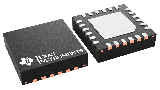
The ADS8201 is available in a 24-lead, 4×4 QFN package, and is specified over the –40°C to +85°C industrial temperature range.


