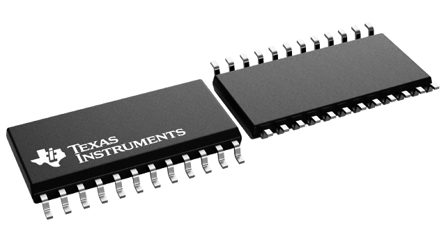
SN74HC646 Series
Octal Bus Transceivers And Registers With 3-State Outputs
Manufacturer: Texas Instruments
Catalog
Octal Bus Transceivers And Registers With 3-State Outputs
Key Features
• Wide Operating Voltage Range of 2 V to 6 VHigh-Current 3-State Outputs Can Drive Up To 15 LSTTL LoadsLow Power Consumption, 80-µA Max ICCTypical tpd= 11 ns±6-mA Output Drive at 5 VLow Input Current of 1 µA MaxIndependent Registers for A and B BusesMultiplexed Real-Time and Stored DataTrue Data PathsWide Operating Voltage Range of 2 V to 6 VHigh-Current 3-State Outputs Can Drive Up To 15 LSTTL LoadsLow Power Consumption, 80-µA Max ICCTypical tpd= 11 ns±6-mA Output Drive at 5 VLow Input Current of 1 µA MaxIndependent Registers for A and B BusesMultiplexed Real-Time and Stored DataTrue Data Paths
Description
AI
The ’HC646 devices consist of bus-transceiver circuits with 3-state outputs, D-type flip-flops, and control circuitry arranged for multiplexed transmission of data directly from the input bus or from the internal registers. Data on the A or B bus is clocked into the registers on the low-to-high transition of the appropriate clock (CLKAB or CLKBA) input. Figure 1 illustrates the four fundamental bus-management functions that can be performed with the ’HC646 devices.
Output-enable (OE)\ and direction-control (DIR) inputs control the transceiver functions. In the transceiver mode, data present at the high-impedance port may be stored in either or both registers.
The select-control (SAB and SBA) inputs can multiplex stored and real-time (transparent mode) data. DIR determines which bus receives data when OE\ is active (low). In the isolation mode (OE\ high), A data may be stored in one register and/or B data may be stored in the other register.
To ensure the high-impedance state during power up or power down, OE\ should be tied to VCCthrough a pullup resistor; the minimum value of the resistor is determined by the current-sinking capability of the driver.
When an output function is disabled, the input function is still enabled and can be used to store data. Only one of the two buses, A or B, may be driven at a time.


