TX7316 Series
16-channel 3-level or 8-channel 5-level transmitter with integrated transmit beamformer
Manufacturer: Texas Instruments
Catalog
16-channel 3-level or 8-channel 5-level transmitter with integrated transmit beamformer
Description
AI
The TX7316 is a highly integrated, high-performance transmitter solution for ultrasound imaging system. The device has total 16 pulser circuits (PULS), 16 transmit/receive (T/R) switches, and supports both on-chip and off-chip beamformer (TxBF). The device also integrates on-chip floating power supplies that reduce the number of required high voltage power supplies.
The TX7316 (referred to as device in this data sheet) has a pulser circuit that generates three-level high voltage pulses (up to ±100 V) that can be used to excite multiple channels of an ultrasound transducer. The device supports total 8 outputs for 5-level mode and 16 outputs for 3-level mode. The maximum output current is configurable from 2.4 A to 0.6 A.
A T/R switch under OFF state protects the receiver circuit by providing high isolation between the high-voltage transmitter and the low-voltage receiver when the pulser is generating high-voltage pulses. When the transducer is receiving echo signals, the T/R switch turns ON and connects the transducer to the receiver. The ON/OFF operation of the T/R switch is either controlled by an external pin or controlled by on-chip beamforming engine in the device. The T/R switch offers 12-Ω impedance in the ON state.
Ultrasound transmission relies on the excitation of multiple transducer elements with the delay profile of the excitation across the different elements defining the direction of the transmission. Such an operation is referred to as transmit beamforming. The TX7316 supports staggered pulsing of the different channels, allowing for transmit beamforming. The device supports both off-chip and on-chip beamforming operation.
In the off-chip beamformer mode, the output transition of each pulser and TR switch ON/OFF operation is controlled by external control pins. To eliminate the effect of jitter from the external control signals, the device supports a synchronization feature. When the synchronization feature is enabled, the external control signals are latched using a low-jitter beamformer clock signal.
In the on-chip beamformer mode, the delay profile for the pulsing of the different channels is stored within the device. The device supports a transmit beamformer delay resolution of one beamformer clock period and a maximum delay of 213beamformer clock periods. An internal pattern generator generates the output pulse patterns based on pattern profiles stored in a profile RAM. Up to 16 beamforming profiles and 48/28 pattern profiles for 3/5-level mode can be stored in the profile RAM. On-chip beamforming mode reduces the number of control signals that must be routed from the FPGA to the device.
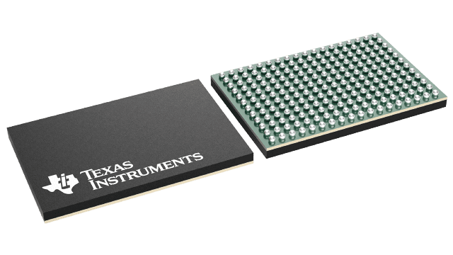
TX7316 is available in a 15-mm × 10-mm 216-pin NFBGA package (ZCX package) and is specified for operation from 0°C to 70°C.


