Catalog
High Speed 3A Synchronous MOSFET Driver
Key Features
• Shoot-Through ProtectionInput Under-Voltage-Lock-Out3A Peak Driving Current195µA Quiescent Current28V Input Voltage in Buck ConfigurationSOIC-8 and WSON PackagesAll trademarks are the property of their respective owners.Shoot-Through ProtectionInput Under-Voltage-Lock-Out3A Peak Driving Current195µA Quiescent Current28V Input Voltage in Buck ConfigurationSOIC-8 and WSON PackagesAll trademarks are the property of their respective owners.
Description
AI
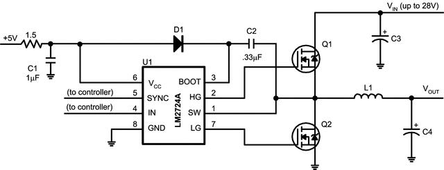
The LM2724A is a dual N-channel MOSFET driver which can drive both the top and bottom MOSFETs in a push-pull structure simultaneously. The LM2724A takes a logic input and splits it into two complimentary signals with a typical 20ns dead time in between. The built-in cross-conduction protection circuitry prevents the top and bottom MOSFETs from turning on simultaneously. With a bias voltage of 5V, the peak sourcing and sinking current for each driver of the LM2724A is about 3A. Input UVLO (Under-Voltage-Lock-Out) ensures that all the driver outputs stay low until the supply rail exceeds the power-on threshold during system power on, or after the supply rail drops below power-on threshold by a specified hysteresis during system power down. The cross-conduction protection circuitry detects both driver outputs and will not turn on a driver until the other driver output is low. The top gate voltage needed by the top MOSFET is obtained through an external boot-strap structure. When not switching, the LM2724A only draws up to 195µA from the 5V rail. The synchronization operation of the bottom MOSFET can be disabled by pulling the SYNC pin to ground.
The LM2724A is a dual N-channel MOSFET driver which can drive both the top and bottom MOSFETs in a push-pull structure simultaneously. The LM2724A takes a logic input and splits it into two complimentary signals with a typical 20ns dead time in between. The built-in cross-conduction protection circuitry prevents the top and bottom MOSFETs from turning on simultaneously. With a bias voltage of 5V, the peak sourcing and sinking current for each driver of the LM2724A is about 3A. Input UVLO (Under-Voltage-Lock-Out) ensures that all the driver outputs stay low until the supply rail exceeds the power-on threshold during system power on, or after the supply rail drops below power-on threshold by a specified hysteresis during system power down. The cross-conduction protection circuitry detects both driver outputs and will not turn on a driver until the other driver output is low. The top gate voltage needed by the top MOSFET is obtained through an external boot-strap structure. When not switching, the LM2724A only draws up to 195µA from the 5V rail. The synchronization operation of the bottom MOSFET can be disabled by pulling the SYNC pin to ground.


