SN74LVC2T45-EP Series
Enhanced Product Dual-Bit Dual Supply Transceiver w/ Configurable Voltage Transl., 3-State Outputs
Manufacturer: Texas Instruments
Catalog
Enhanced Product Dual-Bit Dual Supply Transceiver w/ Configurable Voltage Transl., 3-State Outputs
Key Features
• Available in the Texas Instruments NanoFree™ PackageFully Configurable Dual-Rail Design Allows Each Port toOperate Over the Full 1.65-V to 5.5-V Power-Supply RangeVCCIsolation Feature – If Either VCCInput Is at GND,Both Ports Are in the High-Impedance StateDIR Input Circuit Referenced to VCCALow Power Consumption, 10-µA Max ICC±24-mA Output Drive at 3.3 VIoffSupports Partial-Power-Down Mode OperationMax Data Rates420 Mbps (3.3-V to 5-V Translation)210 Mbps (Translate to 3.3 V)140 Mbps (Translate to 2.5 V)75 Mbps (Translate to 1.8 V)Latch-Up Performance Exceeds 100 mA Per JESD 78, Class IIESD Protection Exceeds JESD 224000-V Human-Body Model (A114-A)200-V Machine Model (A115-A)1000-V Charged-Device Model (C101)SUPPORTS DEFENSE, AEROSPACE, AND MEDICAL APPLICATIONSControlled BaselineOne Assembly/Test SiteOne Fabrication SiteAvailable Temperature Ranges:–55°C to 125°C–55°C to 150°CExtended Product Life CycleExtended Product-Change NotificationProduct TraceabilityNanoFree Is a trademark of Texas InstrumentsAvailable in the Texas Instruments NanoFree™ PackageFully Configurable Dual-Rail Design Allows Each Port toOperate Over the Full 1.65-V to 5.5-V Power-Supply RangeVCCIsolation Feature – If Either VCCInput Is at GND,Both Ports Are in the High-Impedance StateDIR Input Circuit Referenced to VCCALow Power Consumption, 10-µA Max ICC±24-mA Output Drive at 3.3 VIoffSupports Partial-Power-Down Mode OperationMax Data Rates420 Mbps (3.3-V to 5-V Translation)210 Mbps (Translate to 3.3 V)140 Mbps (Translate to 2.5 V)75 Mbps (Translate to 1.8 V)Latch-Up Performance Exceeds 100 mA Per JESD 78, Class IIESD Protection Exceeds JESD 224000-V Human-Body Model (A114-A)200-V Machine Model (A115-A)1000-V Charged-Device Model (C101)SUPPORTS DEFENSE, AEROSPACE, AND MEDICAL APPLICATIONSControlled BaselineOne Assembly/Test SiteOne Fabrication SiteAvailable Temperature Ranges:–55°C to 125°C–55°C to 150°CExtended Product Life CycleExtended Product-Change NotificationProduct TraceabilityNanoFree Is a trademark of Texas Instruments
Description
AI
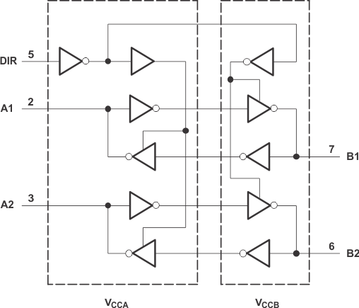
This dual-bit noninverting bus transceiver uses two separate configurable power-supply rails. The A port is designed to track VCCA. VCCAaccepts any supply voltage from 1.65 V to 5.5 V. The B port is designed to track VCCB. VCCBaccepts any supply voltage from 1.65 V to 5.5 V. This allows for universal low-voltage bidirectional translation between any of the 1.8-V, 2.5-V, 3.3-V, and 5-V voltage nodes.
The SN74LVC2T45 is designed for asynchronous communication between two data buses. The logic levels of the direction-control (DIR) input activate either the B-port outputs or the A-port outputs. The device transmits data from the A bus to the B bus when the B-port outputs are activated, and from the B bus to the A bus when the A-port outputs are activated. The input circuitry on both A and B ports always is active and must have a logic HIGH or LOW level applied to prevent excess ICCand ICCZ.
The SN74LVC2T45 is designed so that the DIR input circuit is supplied by VCCA.
This device is fully specified for partial-power-down applications using Ioff. The Ioffcircuitry disables the outputs, preventing damaging current backflow through the device when it is powered down.
The VCCisolation feature ensures that if either VCCinput is at GND, both ports are in the high-impedance state.
NanoFree™ package technology is a major breakthrough in IC packaging concepts, using the die as the package.


