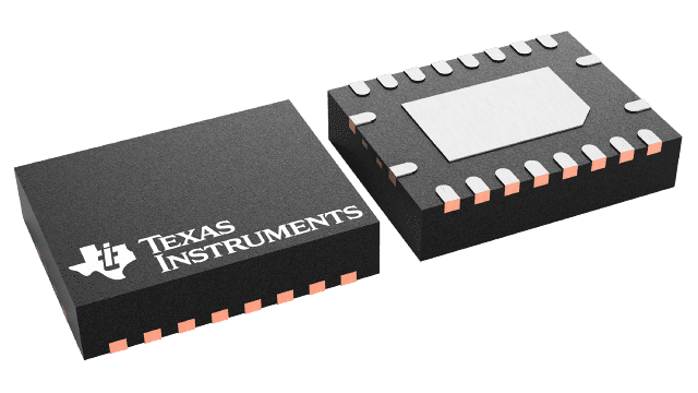
SN74AUC240 Series
8-ch, 0.8-V to 2.7-V high speed inverters with 3-state outputs
Manufacturer: Texas Instruments
Catalog
8-ch, 0.8-V to 2.7-V high speed inverters with 3-state outputs
Key Features
• Optimized for 1.8-V Operation and is 3.6-V I/O Tolerant to Support Mixed-Mode Signal OperationIoffSupports Partial-Power-Down Mode OperationSub 1-V OperableMax tpdof 1.7 ns at 1.8 VLow Power Consumption, 20-µA Max ICC±8-mA Output Drive at 1.8 VLatch-Up Performance Exceeds 100 mA Per JESD 78, Class IIESD Protection Exceeds JESD 222000-V Human-Body Model (A114-A)200-V Machine Model (A115-A)1000-V Charged-Device Model (C101)Optimized for 1.8-V Operation and is 3.6-V I/O Tolerant to Support Mixed-Mode Signal OperationIoffSupports Partial-Power-Down Mode OperationSub 1-V OperableMax tpdof 1.7 ns at 1.8 VLow Power Consumption, 20-µA Max ICC±8-mA Output Drive at 1.8 VLatch-Up Performance Exceeds 100 mA Per JESD 78, Class IIESD Protection Exceeds JESD 222000-V Human-Body Model (A114-A)200-V Machine Model (A115-A)1000-V Charged-Device Model (C101)
Description
AI
This octal buffer/driver is operational at 0.8-V to 2.7-V VCC, but is designed specifically for 1.65-V to 1.95-V VCCoperation.
The SN74AUC240 is designed specifically to improve the performance and density of 3-state memory address drivers, clock drivers, and bus-oriented receivers and transmitters.
This device is organized as two 4-bit buffers/drivers with separate output-enable (OE)\ inputs. When OE\ is low, the device passes data from the A inputs to the Y outputs. When OE\ is high, the outputs are in the high-impedance state.
To ensure the high-impedance state during power up or power down, OE\ should be tied to VCCthrough a pullup resistor; the minimum value of the resistor is determined by the current-sinking capability of the driver.
This device is fully specified for partial-power-down applications using Ioff. The Ioffcircuitry disables the outputs, preventing damaging current backflow through the device when it is powered down.


