Catalog
3.6-V, 4-A, 5.3-mΩ load switch with output discharge
Key Features
• Input Voltage Range: 0.75 V to 3.6 VIntegrated Load SwitchIntegrated Pass-FET rDSON= 2 mΩ (Typ) at 3.6 VTypical ON-ResistancerON= 5.3 mΩ at VIN= 3.6 VrON= 5.4 mΩ at VIN= 2.5 VrON= 5.5 mΩ at VIN= 1.8 VrON= 5.8 mΩ at VIN= 1.2 VrON= 6.1 mΩ at VIN= 1.05 VrON= 7.3 mΩ at VIN= 0.75 VCSP-8 Package 0.9 mm × 1.9 mm, 0.5 mm Pitch4-A Maximum Continuous Switch CurrentShutdown Current 5.5-µA MaxON-Logic Available in Both Active High/Low:TPS22920 is Active HighTPS22920L is Active LowLow Threshold Control InputControlled Slew-Rate to Avoid Inrush CurrentQuick Output Discharge ResistorESD Performance Tested Per JESD 224000-V Human-Body Model(A114-B, Class II)1000-V Charged-Device Model (C101)Input Voltage Range: 0.75 V to 3.6 VIntegrated Load SwitchIntegrated Pass-FET rDSON= 2 mΩ (Typ) at 3.6 VTypical ON-ResistancerON= 5.3 mΩ at VIN= 3.6 VrON= 5.4 mΩ at VIN= 2.5 VrON= 5.5 mΩ at VIN= 1.8 VrON= 5.8 mΩ at VIN= 1.2 VrON= 6.1 mΩ at VIN= 1.05 VrON= 7.3 mΩ at VIN= 0.75 VCSP-8 Package 0.9 mm × 1.9 mm, 0.5 mm Pitch4-A Maximum Continuous Switch CurrentShutdown Current 5.5-µA MaxON-Logic Available in Both Active High/Low:TPS22920 is Active HighTPS22920L is Active LowLow Threshold Control InputControlled Slew-Rate to Avoid Inrush CurrentQuick Output Discharge ResistorESD Performance Tested Per JESD 224000-V Human-Body Model(A114-B, Class II)1000-V Charged-Device Model (C101)
Description
AI
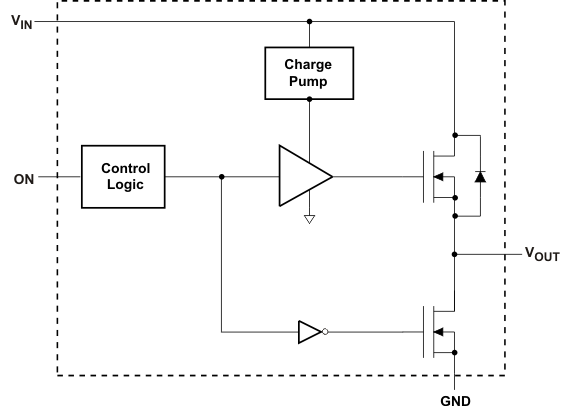
The TPS22920x is a small, space-saving load switch with controlled turn on to reduce inrush current. The device contains a N-channel MOSFET that can operate over an input voltage range of 0.75 V to 3.6 V and switch currents up to 4 A. An integrated charge pump biases the NMOS switch in order to achieve a minimum switch ON resistance (rON). The switch is controlled by an on/off input (ON), which is capable of interfacing directly with low-voltage control signals.
The TPS22920x has a 1250-Ω on-chip resistor for quick output discharge when the switch is turned off which insures that the output is not left floating.
The TPS22920x has an internally controlled rise time in order to reduce inrush current.
The TPS22920x is available in an ultra-small, space- saving 8-pin CSP package and is characterized for operation over the free-air temperature range of –40°C to 85°C.


